Electrical Characteristics
324 Datasheet
NOTE:
1. Refer to note 3 of table 4-4 in Section 4.2.2.2 and note 2 of table 4-6 in Section 4.2.3.2 of
the PCI Local Bus Specification, Revision 2.3 for measurement details.
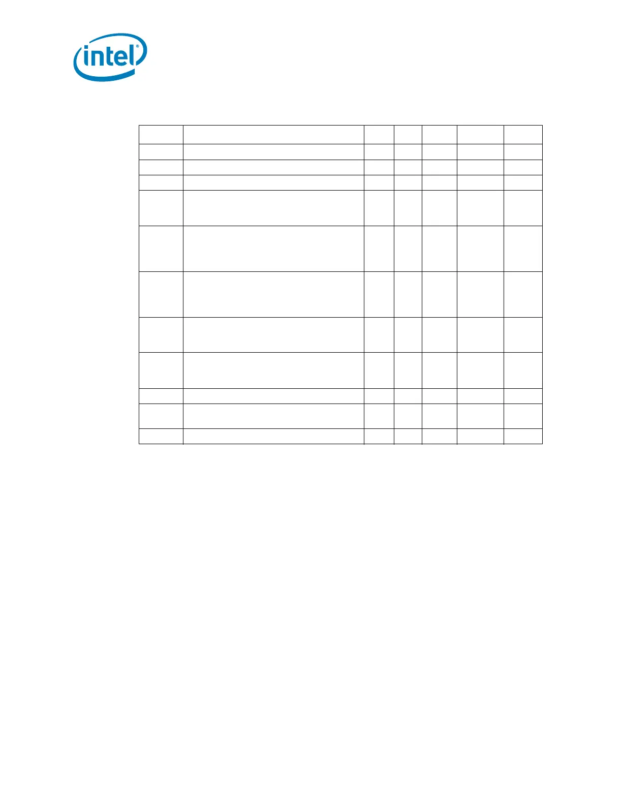
Table 8-25. PCI Interface Timing
Sym Parameter Min Max Units Notes Figure
t40 AD[31:0] Valid Delay 2 11 ns 1 8-12
t41 AD[31:0] Setup Time to PCICLK Rising 7 — ns 8-13
t42 AD[31:0] Hold Time from PCICLK Rising 0 — ns 8-13
t43
C/BE[3:0]#, FRAME#, TRDY#, IRDY#,
STOP#, PAR, PERR#, PLOCK#, DEVSEL#
Valid Delay from PCICLK Rising
211ns 1 8-12
t44
C/BE[3:0]#, FRAME#, TRDY#, IRDY#,
STOP#, PAR, PERR#, PLOCK#, IDSEL,
DEVSEL# Output Enable Delay from
PCICLK Rising
2ns 8-16
t45
C/BE[3:0]#, FRAME#, TRDY#, IRDY#,
STOP#, PERR#, PLOCK#, DEVSEL#,
GNT[A:B]# Float Delay from PCICLK
Rising
228ns 8-14
t46
C/BE[3:0]#, FRAME#, TRDY#, IRDY#,
STOP#, SERR#, PERR#, DEVSEL#, Setup
Time to PCICLK Rising
7ns 8-13
t47
C/BE[3:0]#, FRAME#, TRDY#, IRDY#,
STOP#, SERR#, PERR#, DEVSEL#,
REQ[A:B]# Hold Time from PCLKIN Rising
0—ns 8-13
t48 PCIRST# Low Pulse Width 1 ms 8-15
t49
GNT[3:0]# Valid Delay from PCICLK
Rising
212ns
t50 REQ[3:0]# Setup Time to PCICLK Rising 12 — ns