SATA Controller Registers (D31:F2)
588 Datasheet
14.4 AHCI Registers (D31:F2)
Note: These registers are AHCI-specific and available when the PCH is properly configured.
The Serial ATA Status, Control, and Error registers are special exceptions and may be
accessed on all PCH components if properly configured; see Section 14.3 for details.
The memory mapped registers within the SATA controller exist in non-cacheable
memory space. Additionally, locked accesses are not supported. If software attempts to
perform locked transactions to the registers, indeterminate results may occur. Register
accesses shall have a maximum size of 64-bits; 64-bit access must not cross an 8-byte
alignment boundary. All memory registers are reset by Function Level Reset unless
specified otherwise.
The registers are broken into two sections – generic host control and port control. The
port control registers are the same for all ports, and there are as many registers banks
as there are ports.
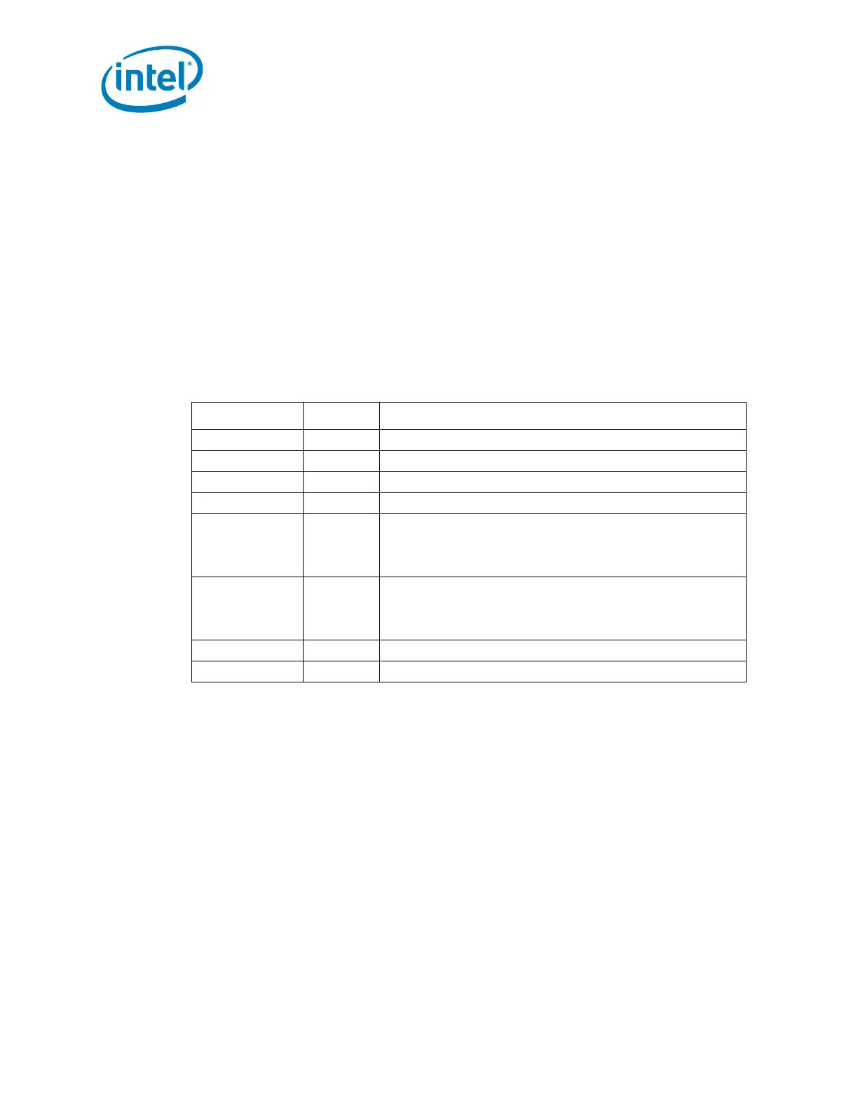
Table 14-3. AHCI Register Address Map
ABAR + Offset Mnemonic Register
00–1Fh GHC Generic Host Control
20h–FFh — Reserved
100h–17Fh P0PCR Port 0 port control registers
180h–1FFh P1PCR Port 1 port control registers
200h–27Fh P2PCR
Port 2 port control registers
NOTE: Registers may be Reserved depending on if port is
available in the given SKU. See Section 1.3 for details if
port is available.
280h–2FFh P3PCR
Port 3 port control registers
NOTE: Registers may be Reserved depending on if port is
available in the given SKU. See Section 1.3 for details if
port is available.
300h–37Fh P4PCR Port 4 port control registers
380h–3FFh P5PCR Port 5 port control registers
 Loading...
