SMBus Controller Registers (D31:F3)
746 Datasheet
18.2 SMBus I/O and Memory Mapped I/O Registers
The SMBus registers (see Table 18-2) can be accessed through I/O BAR or Memory BAR
registers in PCI configuration space. The offsets are the same for both I/O and Memory
Mapped I/O registers.
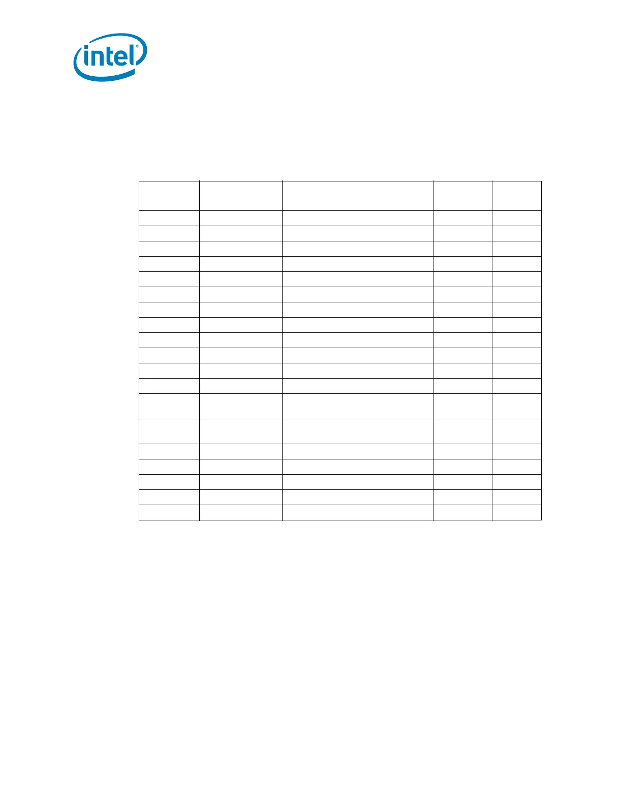
Table 18-2. SMBus I/O and Memory Mapped I/O Register Address Map
SMB_BASE
+ Offset
Mnemonic Register Name Default Type
00h HST_STS Host Status 00h R/WC, RO
02h HST_CNT Host Control 00h R/W, WO
03h HST_CMD Host Command 00h R/W
04h XMIT_SLVA Transmit Slave Address 00h R/W
05h HST_D0 Host Data 0 00h R/W
06h HST_D1 Host Data 1 00h R/W
07h HOST_BLOCK_DB Host Block Data Byte 00h R/W
08h PEC Packet Error Check 00h R/W
09h RCV_SLVA Receive Slave Address 44h R/W
0Ah–0Bh SLV_DATA Receive Slave Data 0000h RO
0Ch AUX_STS Auxiliary Status 00h R/WC, RO
0Dh AUX_CTL Auxiliary Control 00h R/W
0Eh SMLINK_PIN_CTL
SMLink Pin Control (TCO
Compatible Mode)
See register
description
R/W, RO
0Fh SMBus_PIN_CTL SMBus Pin Control
See register
description
R/W, RO
10h SLV_STS Slave Status 00h R/WC
11h SLV_CMD Slave Command 00h R/W
14h NOTIFY_DADDR Notify Device Address 00h RO
16h NOTIFY_DLOW Notify Data Low Byte 00h RO
17h NOTIFY_DHIGH Notify Data High Byte 00h RO