Datasheet 617
SATA Controller Registers (D31:F5)
15 SATA Controller Registers
(D31:F5)
15.1 PCI Configuration Registers (SATA–D31:F5)
Note: Address locations that are not shown should be treated as Reserved.
All of the SATA registers are in the core well. None of the registers can be locked.
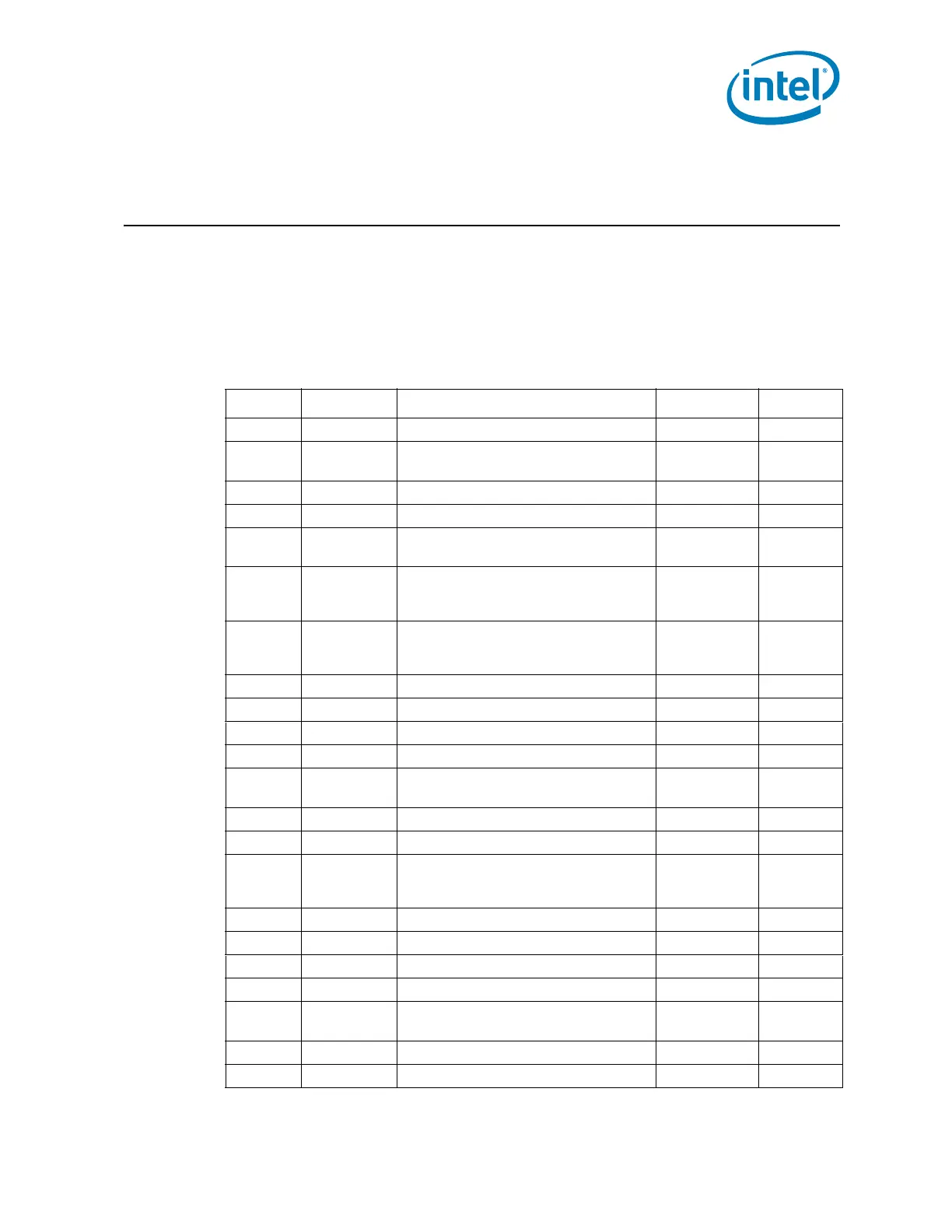
Table 15-1. SATA Controller PCI Register Address Map (SATA–D31:F5) (Sheet 1 of 2)
Offset Mnemonic Register Name Default Type
00h–01h VID Vendor Identification 8086h RO
02h–03h DID Device Identification
See register
description
RO
04h–05h PCICMD PCI Command 0000h R/W, RO
06h–07h PCISTS PCI Status 02B0h R/WC, RO
08h RID Revision Identification
See register
description
RO
09h PI Programming Interface
See register
description
See
register
description
0Ah SCC Sub Class Code
See register
description
See
register
description
0Bh BCC Base Class Code 01h RO
0Dh PMLT Primary Master Latency Timer 00h RO
10h–13h PCMD_BAR Primary Command Block Base Address 00000001h R/W, RO
14h–17h PCNL_BAR Primary Control Block Base Address 00000001h R/W, RO
18h–1Bh SCMD_BAR
Secondary Command Block Base
Address
00000001h R/W, RO
1Ch–1Fh SCNL_BAR Secondary Control Block Base Address 00000001h R/W, RO
20h–23h BAR Legacy Bus Master Base Address 00000001h R/W, RO
24h–27h SIDPBA
Serial ATA Index / Data Pair Base
Address
00000000h
See
register
description
2Ch–2Dh SVID Subsystem Vendor Identification 0000h R/WO
2Eh–2Fh SID Subsystem Identification 0000h R/WO
34h CAP Capabilities Pointer 80h RO
3Ch INT_LN Interrupt Line 00h R/W
3Dh INT_PN Interrupt Pin
See register
description
RO
40h–41h IDE_TIM Primary IDE Timing Register 0000h R/W
42h–43h IDE_TIM Secondary IDE Timing Registers 0000h R/W