SATA Controller Registers (D31:F5)
618 Datasheet
NOTE: The PCH SATA controller is not arbitrated as a PCI device; therefore, it does not need a
master latency timer.
15.1.1 VID—Vendor Identification Register (SATA—D31:F5)
Offset Address: 00h–01h Attribute: RO
Default Value: 8086h Size: 16 bit
Lockable: No Power Well: Core
15.1.2 DID—Device Identification Register (SATA—D31:F5)
Offset Address: 02h–03h Attribute: RO
Default Value: See bit description Size: 16 bit
Lockable: No Power Well: Core
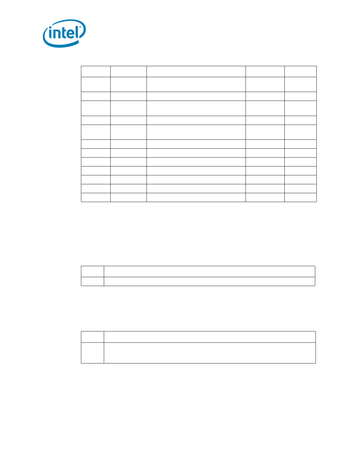
70h–71h PID PCI Power Management Capability ID
See register
description
RO
72h–73h PC PCI Power Management Capabilities 4003h RO
74h–75h PMCS
PCI Power Management Control and
Status
0008h
R/W, RO,
R/WC
90h MAP Address Map 00h R/W
92h–93h PCS Port Control and Status 0000h
R/W, RO,
R/WC
A8h–ABh SATACR0 SATA Capability Register 0 0010B012h RO
ACh–AFh SATACR1 SATA Capability Register 1 00000048h RO
B0h–B1h FLRCID FLR Capability ID 0009h RO
B2h–B3h FLRCLV FLR Capability Length and Value 2006h RO
B4h–B5h FLRCTRL FLR Control 0000h R/W, RO
C0h ATC APM Trapping Control 00h R/W
C4h ATS ATM Trapping Status 00h R/WC
Table 15-1. SATA Controller PCI Register Address Map (SATA–D31:F5) (Sheet 2 of 2)
Offset Mnemonic Register Name Default Type
Bit Description
15:0 Vendor ID — RO. This is a 16-bit value assigned to Intel. Intel VID = 8086h
Bit Description
15:0
Device ID — RO. This is a 16-bit value assigned to the PCH SATA controller.
NOTE: The value of this field will change dependent upon the value of the MAP
Register. See Section and Section 15.1.25