Datasheet 757
PCI Express* Configuration Registers
19 PCI Express* Configuration
Registers
19.1 PCI Express* Configuration Registers
(PCI Express*—D28:F0/F1/F2/F3/F4/F5/F6/F7)
Note: This section assumes the default PCI Express Function Number-to-Root Port mapping is
used. Function numbers for a given root port are assignable through the Root Port
Function Number and Hide for PCI Express Root Ports registers (RCBA+0404h).
Note: Register address locations that are not shown in Table 19-1, should be treated as
Reserved.
/
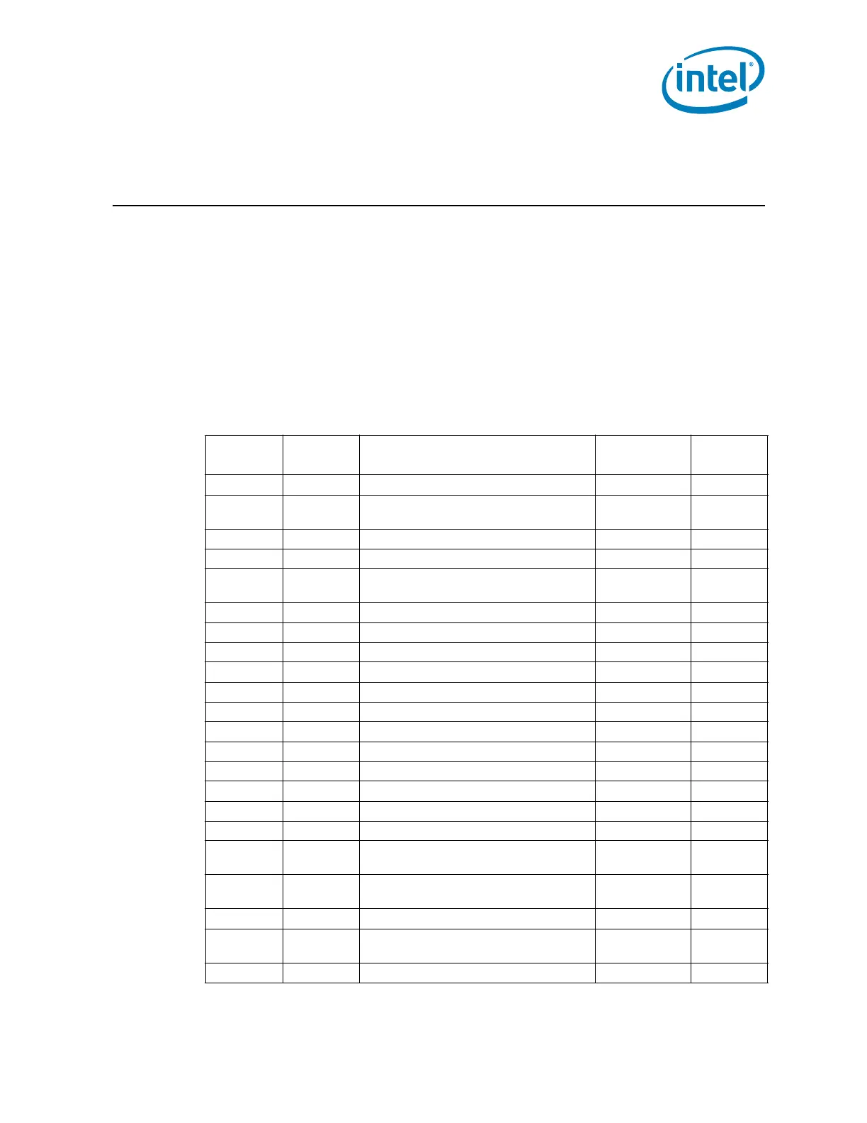
Table 19-1. PCI Express* Configuration Registers Address Map
(PCI Express*—D28:F0/F1/F2/F3/F4/F5/F6/F7) (Sheet 1 of 3)
Offset Mnemonic Register Name
Function 0–5
Default
Type
00h–01h VID Vendor Identification 8086h RO
02h–03h DID Device Identification
See register
description
RO
04h–05h PCICMD PCI Command 0000h R/W, RO
06h–07h PCISTS PCI Status 0010h R/WC, RO
08h RID Revision Identification
See register
description
RO
09h PI Programming Interface 00h RO
0Ah SCC Sub Class Code 04h RO
0Bh BCC Base Class Code 06h RO
0Ch CLS Cache Line Size 00h R/W
0Dh PLT Primary Latency Timer 00h RO
0Eh HEADTYP Header Type 81h RO
18h–1Ah BNUM Bus Number 000000h R/W
1Bh SLT Secondary Latency Timer 00h RO
1Ch–1Dh IOBL I/O Base and Limit 0000h R/W, RO
1Eh–1Fh SSTS Secondary Status Register 0000h R/WC
20h–23h MBL Memory Base and Limit 00000000h R/W
24h–27h PMBL Prefetchable Memory Base and Limit 00010001h R/W, RO
28h–2Bh PMBU32
Prefetchable Memory Base Upper 32
Bits
00000000h R/W
2Ch–2Fh PMLU32
Prefetchable Memory Limit Upper 32
Bits
00000000h R/W
34h CAPP Capabilities List Pointer 40h RO
3Ch–3Dh INTR Interrupt Information
See bit
description
R/W, RO
3Eh–3Fh BCTRL Bridge Control Register 0000h R/W