Electrical Characteristics
316 Datasheet
same as the mean. The jitter median describes the point in time where the number of jitter
points on either side is approximately equal as opposed to the averaged time value.
3. Specified at the measurement point and measured over any 250 consecutive UIs. The test
load documented in the PCI Express* specification 2.0 should be used as the RX device
when taking measurements (also refer to the Receiver compliance eye diagram). If the
clocks to the RX and TX are not derived from the same reference clock, the TX UI
recovered from 3500 consecutive UI must be used as a reference for the eye diagram.
4. A T
RX-EYE
= 0.40 UI provides for a total sum of 0.60 UI deterministic and random jitter
budget for the Transmitter and interconnect collected any 250 consecutive UIs. The T
RX-
EYE-MEDIAN-to--MAX-JITTER
specification ensures a jitter distribution in which the median and
the maximum deviation from the median is less than half of the total 0.6 UI jitter budget
collected over any 250 consecutive TX UIs. It should be noted that the median is not the
same as the mean. The jitter median describes the point in time where the number of jitter
points on either side is approximately equal as opposed to the averaged time value. If the
clocks to the RX and TX are not derived from the same reference clock, the TX UI
recovered from 3500 consecutive UI must be used as the reference for the eye diagram.
5. Nominal Unit Interval for highest SDVO speed is 370 ps. However, depending on the
resolution on the interface, the UI may be more than 370 ps.
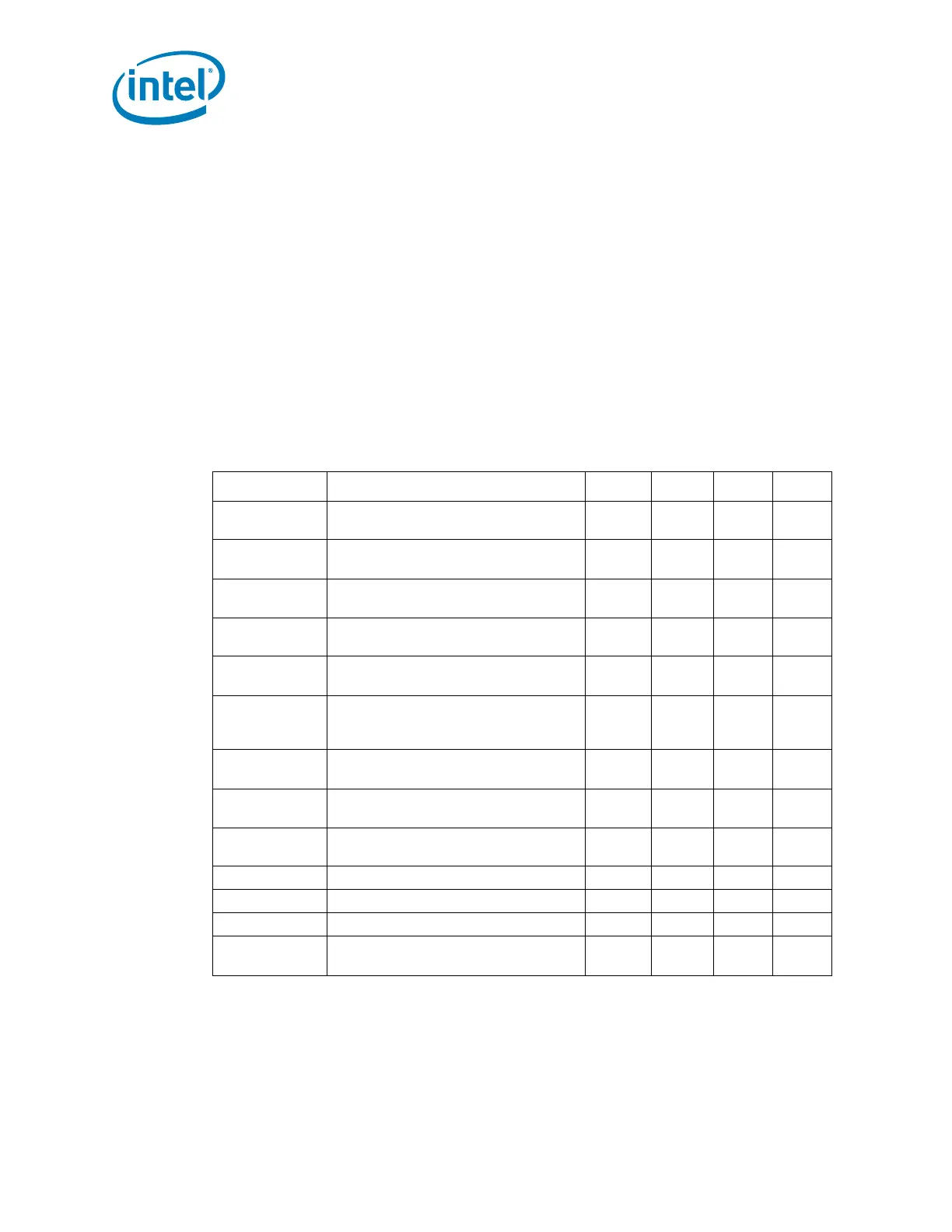
Table 8-19. DisplayPort Interface Timings (DDP[D:B][3:0])
Symbol Parameter Min Nom Max Unit
UI_High_Rate
Unit Interval for High Bit Rate
(2.7 Gbps/lane)
370 — ps
UI_Low_Rate
Unit Interval for Reduced Bit Rate
(1.62 Gbps/lane)
617 — ps
Down_Spread_
Amplitude
Link clock down spreading 0 — 0.5 %
Down_Spread_
Frequency
Link clock down-spreading frequency 30 — 33 kHz
Ltx-skew-
intrapair
Lane Intra-pair output skew at Tx
package pins
—20ps
Ttx-rise/
fall_mismatch_
chipdiff
Lane Intra-pair Rise/Fall time
mismatch at Tx package pin
5%—
V
TX-DIFFp-p-level1
Differential Peak-to-peak Output
Voltage level 1
0.34 0.4 0.46 V
V
TX-DIFFp-p-level2
Differential Peak-to-peak Output
Voltage level 2
0.51 0.6 0.68 V
V
TX-DIFFp-p-level3
Differential Peak-to-peak Output
Voltage level 3
0.69 0.8 0.92 V
V
TX-preemp_ratio
No Pre-emphasis 0 0 0 dB
V
TX-preemp_ratio
3.5 dB Pre-emphasis Level 2.8 3.5 4.2 dB
V
TX-preemp_ratio
6.0 dB Pre-emphasis Level 4.8 6 7.2 dB
L
TX-SKEW-
INTER_PAIR
Lane-to-Lane Output Skew at Tx
package pins
——2UI
 Loading...
