Datasheet 313
Electrical Characteristics
6. INL and DNL measured and calculated according to VESA video signal standards.
7. Max full-scale voltage difference among R,G,B outputs (percentage of steady-state full-scale voltage).
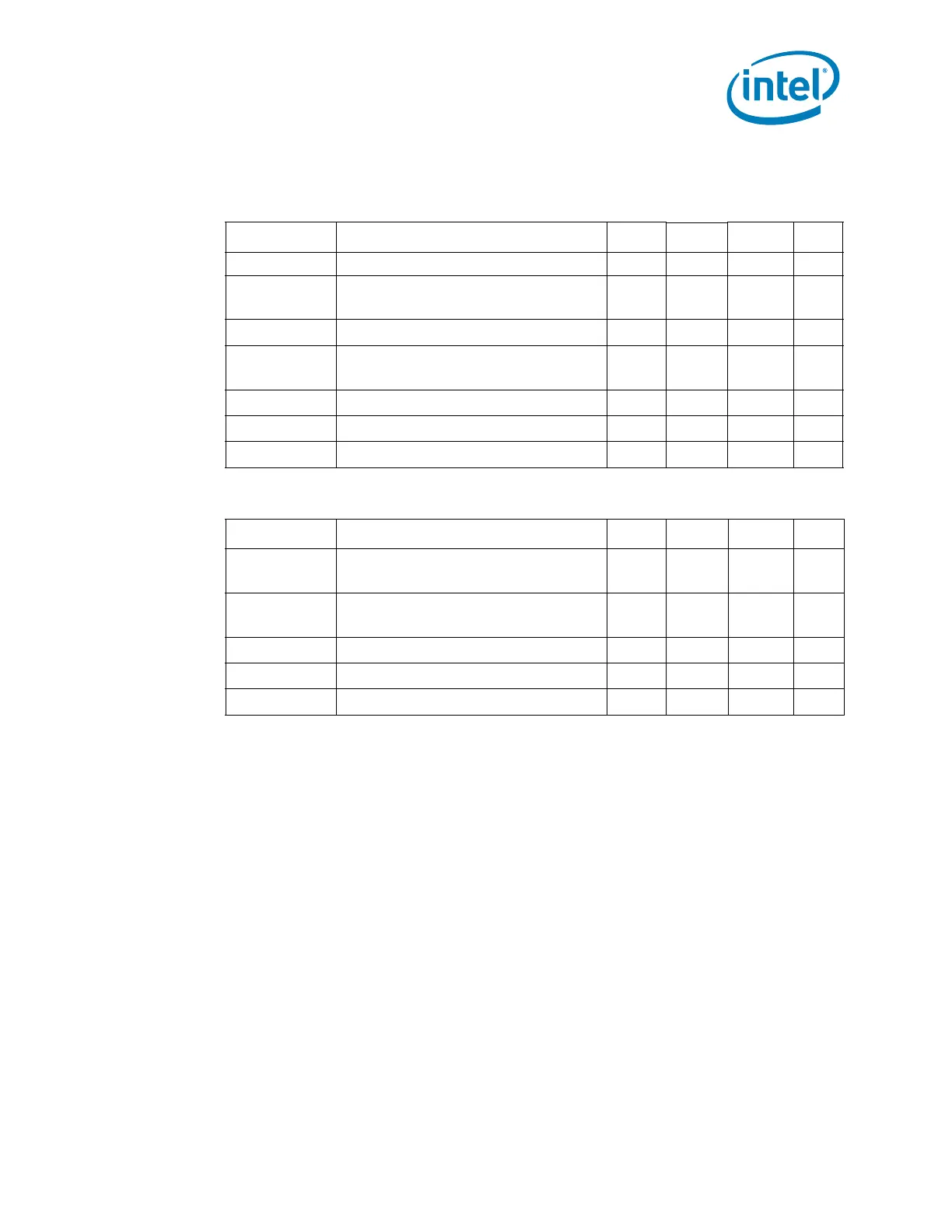
Table 8-14. LVDS Interface: Functional Operating Range (VccALVDS = 1.8 V ±5%)
Symbol Parameter Min Nom Max Unit
VOD Differential Output Voltage 250 350 450 mV
VOD
Change in VOD between Complementary
Output States
——50mV
VOS
Offset Voltage
1.125 1.25 1.375 V
VOS
Change in VOS between Complementary
Output States
——50mV
IOs
Output Short Circuit Current
—-3.5-10mA
IOZ
Output TRI-STATE Current
— ±1 ±10 µA
Vcm(ac)
AC Common Mode noise
150 mV
Table 8-15. Display Port Auxiliary Signal Group DC Characteristics
Symbol Parameter Min Nom Max Unit
Vaux-diff-p-p
Aux peak-to-peak voltage at a transmit-
ting devices
0.39 — 1.38 V
Aux peak-to-peak voltage at a receiving
devices
0.32 — 1.36 V
Vaux-term-R
AUX CH termination DC resistance
—100 —
V-aux-dc-cm
AUX DC common mode voltage
0— 2V
V-aux_turn-CM
Aux turn around common mode voltage
—0.4 V