Datasheet 91
Signal Description
NOTE: See Section 3.1 for full details on pull-up/pull-down resistors.
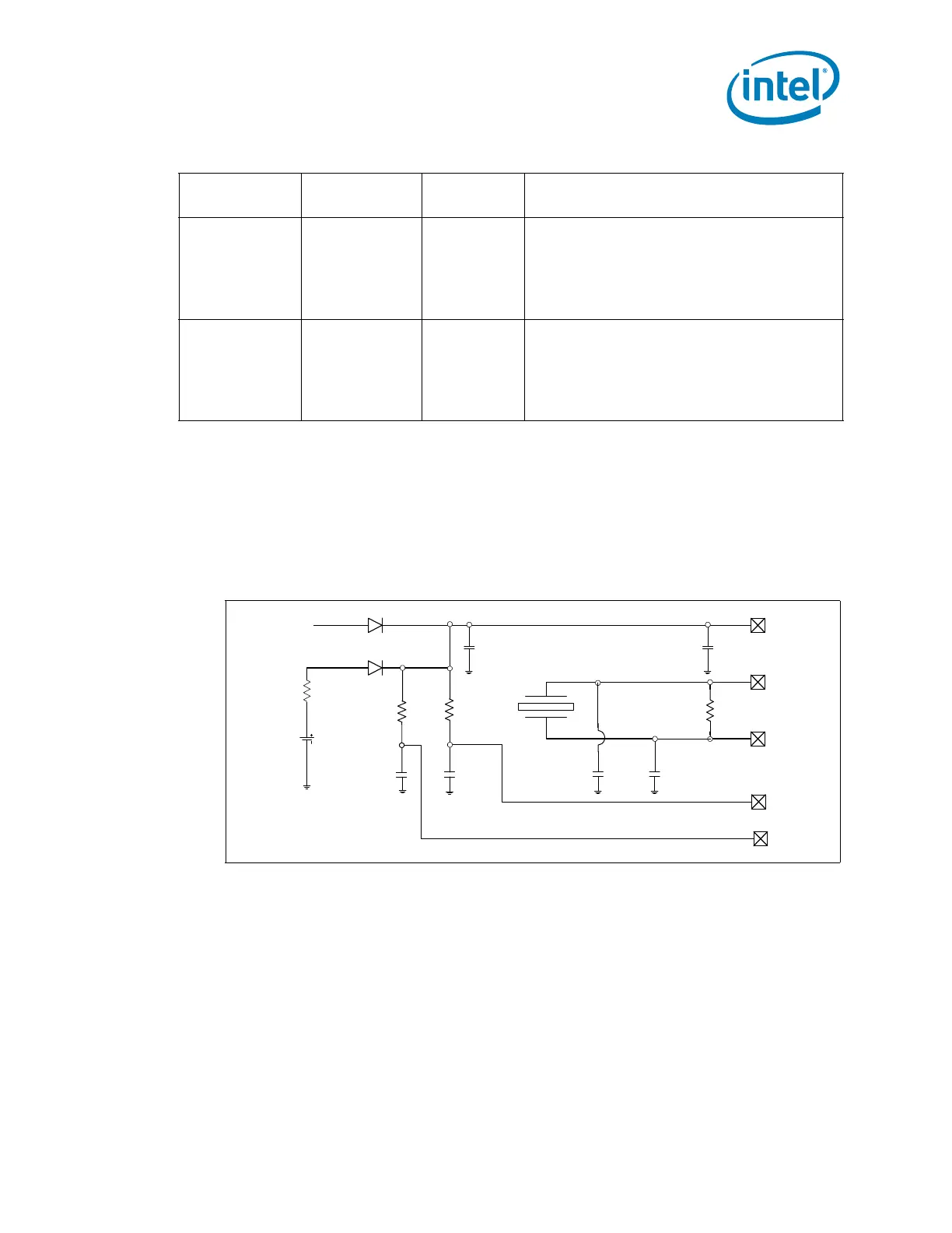
2.28 External RTC Circuitry
The PCH implements an internal oscillator circuit that is sensitive to step voltage
changes in VccRTC. Figure 2-2 shows an example schematic recommended to ensure
correct operation of the PCH RTC.
NOTES:
1. The exact capacitor values for C1 and C2 must be based on the crystal maker
recommendations.
2. Reference designators are arbitrarily assigned.
3. For platforms not supporting Deep S4/S5, the VccDSW3_3 pins will be connected to the
VccSus3_3 pins.
4. Vbatt is voltage provided by the RTC battery (such as coin cell).
5. VccRTC, RTCX1, RTCX2, RTCRST#, and SRTCRST# are PCH pins.
6. VccRTC powers PCH RTC well.
7. RTCX1 is the input to the internal oscillator.
8. RTCX2 is the amplified feedback for the external crystal.
§ §
SATA2GP/GPIO36 Reserved
Rising edge of
PWROK
This signal has a weak internal pull-down.
NOTES:
1. The internal pull-down is disabled after
PLTRST# deasserts.
2. This signal should not be pulled high
when strap is sampled.
SATA3GP/GPIO37 Reserved
Rising edge of
PWROK
This signal has a weak internal pull-down.
NOTES:
1. The internal pull-down is disabled after
PLTRST# deasserts.
2. This signal should not be pulled high
when strap is sampled.
Table 2-27. Functional Strap Definitions (Sheet 5 of 5)
Signal Usage
When
Sampled
Comment
Figure 2-2. Example External RTC Circuit
32.768 KHz
Xtal
10M
VCCRTC
RTCX2
RTCX1
Vbatt
1uF
1 K
VccDSW3_3
(see note 3)
C1 C2
R1
RTCRST#
1.0 uF
20 K
0.1uF
SRTCRST#
20 K
1.0 uF
Schottky Diodes