Electrical Characteristics
320 Datasheet
NOTES:
1. Measured at each R, G, B termination according to the VESA Test Procedure – Evaluation of Analog Display
Graphics Subsystems Proposal (Version 1, Draft 4, December 1, 2000).
2. R, G, B Max Video Rise/Fall Time: 50% of minimum pixel clock period.
3. R, G, B Min Video Rise/Fall Time: 10% of minimum pixel clock period.
4. Max settling time: 30% of minimum pixel clock period.
5. Video channel-channel output skew: 25% of minimum pixel clock period.
6. Overshoot/undershoot: ±12% of black-white video level (full-scale) step function.
7. Noise injection ratio: 2.5% of maximum luminance voltage (dc to max. pixel frequency).
8. R, G, B AC parameters are strongly dependent on the board implementation
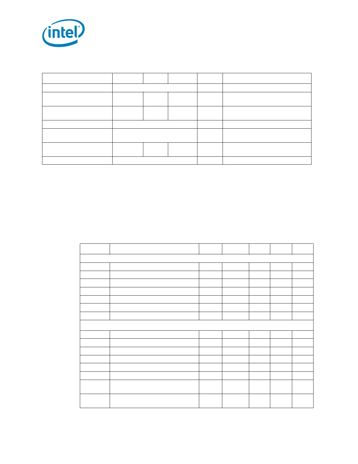
Table 8-23. CRT DAC AC Characteristics
Parameter Min Nom Max Units Notes
Pixel Clock Frequency 400 MHz
R, G, B Video Rise Time 0.25 — 1.25 ns
1, 2, 8 (10-90% of black-to-white
transition, @ 400-MHz pixel clock)
R, G, B Video Fall Time 0.25 — 1.25 ns
1, 3, 8 (90-10% of white-to-black
transition, @ 400-MHz pixel clock)
Settling Time 0.75 ns 1, 4, 8 @ 400-MHz pixel clock
Video channel-to-channel
output skew
0.625 ns 1, 5, 8 @ 400-MHz pixel clock
Overshoot/ Undershoot -0.084 — +0.084 V
1, 6, 8 Full-scale voltage step of
0.7 V
Noise Injection Ratio 2.5 % 1, 7, 8
Table 8-24. Clock Timings (Sheet 1 of 4)
Sym Parameter Min Max
Unit
Notes Figure
PCI Clock (CLKOUT_PCI[4:0])
t1 Period 29.566 30.584 ns 8-11
t2 High Time 10.826 17.850 ns 8-11
t3 Low Time 10.426 17.651 ns 8-11
Duty Cycle 40 60 %
t4 Rising Edge Rate 1.0 4 V/ns 8-11
t5 Falling Edge Rate 1.0 4 V/ns 8-11
Jitter — 500 ps 8,9
14.318 MHz Flex Clock
t6 Period 68.83 70.84 ns 8-11
t7 High Time 29.55 39.00 ns 8-11
t8 Low Time 29.16 38.80 ns 8-11
Duty Cycle 40 60 %
- Rising Edge Rate 1.0 4 V/ns 5
- Falling Edge Rate 1.0 4 V/ns 5
Jitter (14.318 MHz configured on
CLKOUTFLEX1 or CLKOUTFLEX3)
— 800 ps 8,9
Jitter(14.318 MHz configured on
CLKOUTFLEX0 or CLKOUTFLEX2)
—1000ps8,9