Datasheet 331
Electrical Characteristics
8.7 Power Sequencing and Reset Signal Timings
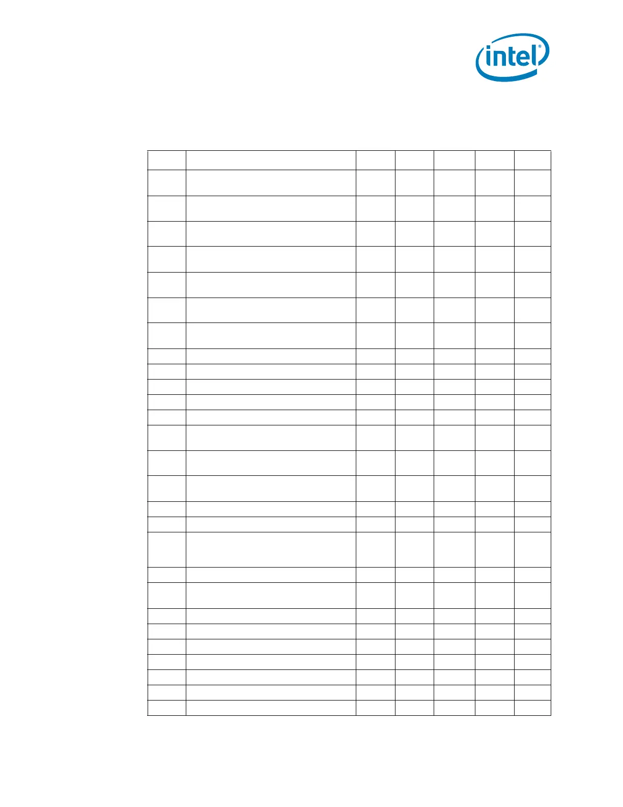
Table 8-36. Power Sequencing and Reset Signal Timings (Sheet 1 of 2)
Sym Parameter Min Max Units Notes Fig
t200 VccRTC active to RTCRST# deassertion 9 — ms
8-1,
8-2
t200a RTCRST# deassertion to DPWROK high 0 — ms
8-1,
8-2
t200b VccDSW3_3 active to DPWROK high 10 — ms
8-1,
8-2
t200c VccDSW3_3 active to VccSus3_3 active 0 — ms
8-1,
8-2
t201 VccSUS active to RSMRST# deassertion 10 — ms 1
8-1,
8-2
t202
DPWROK high to SLP_SUS#
deassertion
95 — ms 2, 3
8-1,
8-2
t202a
RSMRST# and SLP_SUS# deassertion
to SUSCLK toggling
5—ms3, 4
8-1,
8-2
t203 SLP_S5# high to SLP_S4# high 30 µs 5 8-3
t204 SLP_S4# high to SLP_S3# high 30 µs 6 8-3
t205 Vcc active to PWROK high 10 — ms 7, 13
t206 PWROK deglitch time 1 — ms 8
t207 VccASW active to APWROK high 1 — ms
t208
PWROK high to PCH clock outputs
stable
1—ms9
t210
PROCPWRGD and SYS_PWROK high to
SUS_STAT# deassertion
1—ms
t211
SUS_STAT# deassertion to PLTRST#
deassertion
60 — µs
t212 APWROK high to SPI Soft-Start Reads 500 — µs 21
t213 APWROK high to CL_RST1# deasserted 500 — µs 10
t214
DMI message and all PCI Express ports
and DMI in L2/L3 state to SUS_STAT#
active
60 — µs 8-6
t215 SUS_STAT# active to PLTRST# active 210 — µs 8-6
t217
PLTRST# active to PROCPWRGD
inactive
30 — µs 8-6
t218 PROCPWRGD inactive to clocks invalid 10 — µs 8-6
t219 Clocks invalid to SLP_S3# assertion 1 — µs 8-6
t220 SLP_S3# low to SLP_S4# low 30 — µs 8-6
t221 SLP_S4# low to SLP_S5# low 30 — µs 8-6
t222 SLP_S3# active to PWROK deasserted 0 — 8-6
t223 PWROK rising to DRAMPWROK rising 0 — µs 8-8
t224 DRAMPWROK falling to SLP_S4# falling -100 — ns 11 8-8