Electrical Characteristics
310 Datasheet
NOTES:
1. The SERR#, PIRQ[H:A], SMBDATA, SMBCLK, SML[1:0]CLK, SML[1:0]DATA, SML[1:0]ALERT# signals has
an open-drain driver and SATALED# has an open-collector driver, and the V
OH
specification does not apply.
This signal must have external pull-up resistor.
2. PCI Express mVdiff p-p = 2*|PETp[x] – PETn[x]|
3. SATA Vdiff, tx (V
OMIN7
/V
OMAX7
) is measured at the SATA connector on the transmit side (generally, the
motherboard connector), where SATA mVdiff p-p = 2*|SATA[x]TXP – SATA[x]TXN|
4. Maximum Iol for PROCPWRGD is 12mA for short durations (<500 mS per 1.5 s) and 9 mA for long
durations.
5. For INIT3_3V only, for low current devices, the following applies: V
OL5
Max is 0.15 V at an I
OL5
of 2 mA.
6. 3.3 V refers to VccSus3_3 for signals in the suspend well, to Vcc3_3 for signals in the core well, to
VccDSW3_3 for those signals in the Deep S4/S5 well. See Table 3-2 or Table 3-3 for signal and power well
association.
7. 3.3 V refers to VccSus3_3 for signals in the suspend well, to Vcc3_3 for signals in the core well,
VccDSW3_3 for signals in the Deep S4/S5 well. See Table 3-2, or Table 3-3 for signal and power well
association.
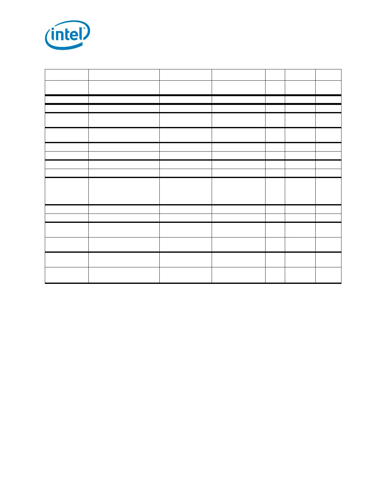
VOH_PECI
Output High Voltage
0.75 ×
V_PROC_IO
V_PROC_IO -6 mA
VOL_HDA Output Low Voltage — 0.1 × VccHDA V 1.5 mA
VOL_JTAG Output Low Voltage 0 0.1 × 1.05 V V 1.5 mA
V_CLKOUT_swi
ng
Differential Output Swing 300 — mV
V_CLKOUT_cro
ss
Clock Cross-Over point 300 550 mV
V_CLKOUTMIN
Min output Voltage -0.3 — V
V_CLKOUTMAX
Max output Voltage 1.15 V V
VOL_PCICLK
Output Low Voltage — 0.4 V -1 mA
VOH_PCICLK
Output High Voltage 2.4 — V 1 mA
VAUX-Diff-P-P
Digital Display Port
Auxiliary Signal peak-to-
peak voltage at
transmitting device
0.39 1.38
Vdiffp
-p
VOL_FDI
Output Low Voltage -.1 0.2 × 3.3 V V 4.1 mA 7
VOH_FDI
Output High Voltage 0.8 × 3.3 V 1.2 V 4.1 mA 7
V
OMIN10-
Gen3i
Minimum Output Voltage 200 —
mVdif
fp-p
3
V
OMAX10-
Gen3i
Maximum Output Voltage — 900
mVdif
fp-p
3
V
OMIN11-
PCIeGen12
Output Low Voltage 800 —
mVdif
fp-p
2
V
OMAX11-
PCIeGen12
Output High Voltage — 1200
mVdif
fp-p
2
Table 8-10. DC Output Characteristics (Sheet 2 of 2)
Symbol Parameter Min Max Unit I
OL /
I
OH
Notes