EHCI Controller Registers (D29:F0, D26:F0)
642 Datasheet
Note: All configuration registers in this section are in the core well and reset by a core well
reset and the D3-to-D0 warm reset, except as noted.
16.1.1 VID—Vendor Identification Register
(USB EHCI—D29:F0, D26:F0)
Offset Address: 00h–01h Attribute: RO
Default Value: 8086h Size: 16 bits
16.1.2 DID—Device Identification Register
(USB EHCI—D29:F0, D26:F0)
Offset Address: 02h–03h Attribute: RO
Default Value: See bit description Size: 16 bits
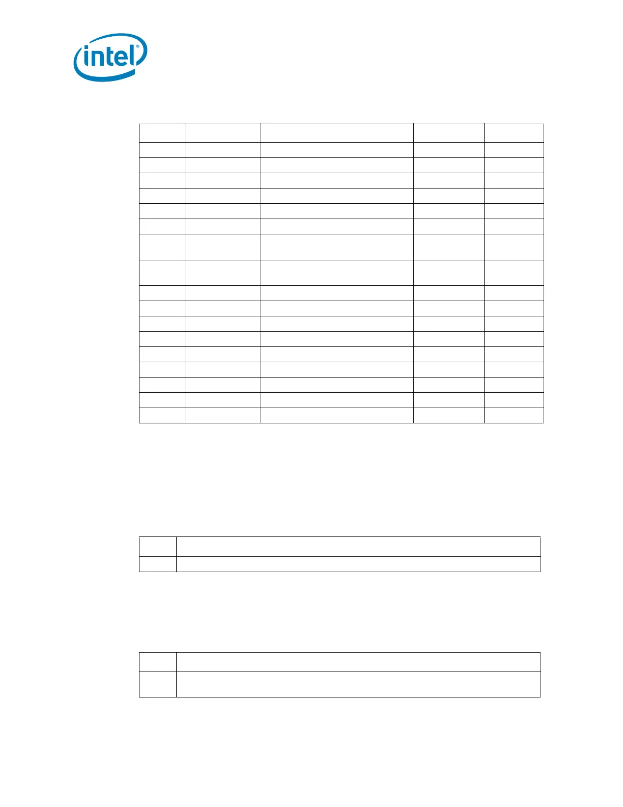
59h NXT_PTR2 Next Item Pointer #2 98h RO
5Ah–5Bh DEBUG_BASE Debug Port Base Offset 20A0h RO
60h USB_RELNUM USB Release Number 20h RO
61h FL_ADJ Frame Length Adjustment 20h R/W
62h–63h PWAKE_CAP Port Wake Capabilities 01FFh R/W
64h–67h — Reserved — —
68h–6Bh LEG_EXT_CAP
USB EHCI Legacy Support
Extended Capability
00000001h R/W, RO
6Ch–6Fh LEG_EXT_CS
USB EHCI Legacy Extended
Support Control/Status
00000000h
R/W, R/WC,
RO
70h–73h SPECIAL_SMI Intel Specific USB 2.0 SMI 00000000h R/W, R/WC
74h–7Fh — Reserved — —
80h ACCESS_CNTL Access Control 00h R/W
84h EHCIIR1 EHCI Initialization Register 1 01h R/W, R/WL
98h FLR_CID FLR Capability ID 09h RO
99h FLR_NEXT FLR Next Capability Pointer 00h RO
9Ah–9Bh FLR_CLV FLR Capability Length and Version 2006h RO, R/WO
9Ch FLR_CTRL FLR Control 00h R/W
9Dh FLR_STAT FLR Status 00h RO
Table 16-1. USB EHCI PCI Register Address Map (USB EHCI—D29:F0, D26:F0) (Sheet 2 of
2)
Offset Mnemonic Register Name Default Value Type
Bit Description
15:0 Vendor ID — RO. This is a 16-bit value assigned to Intel.
Bit Description
15:0
Device ID — RO. This is a 16-bit value assigned to the PCH USB EHCI controller. See
the Intel
®
6 Series Chipset Specification Update for the value of the DID Register.