Rev. 1.50, 10/04, page 156 of 448
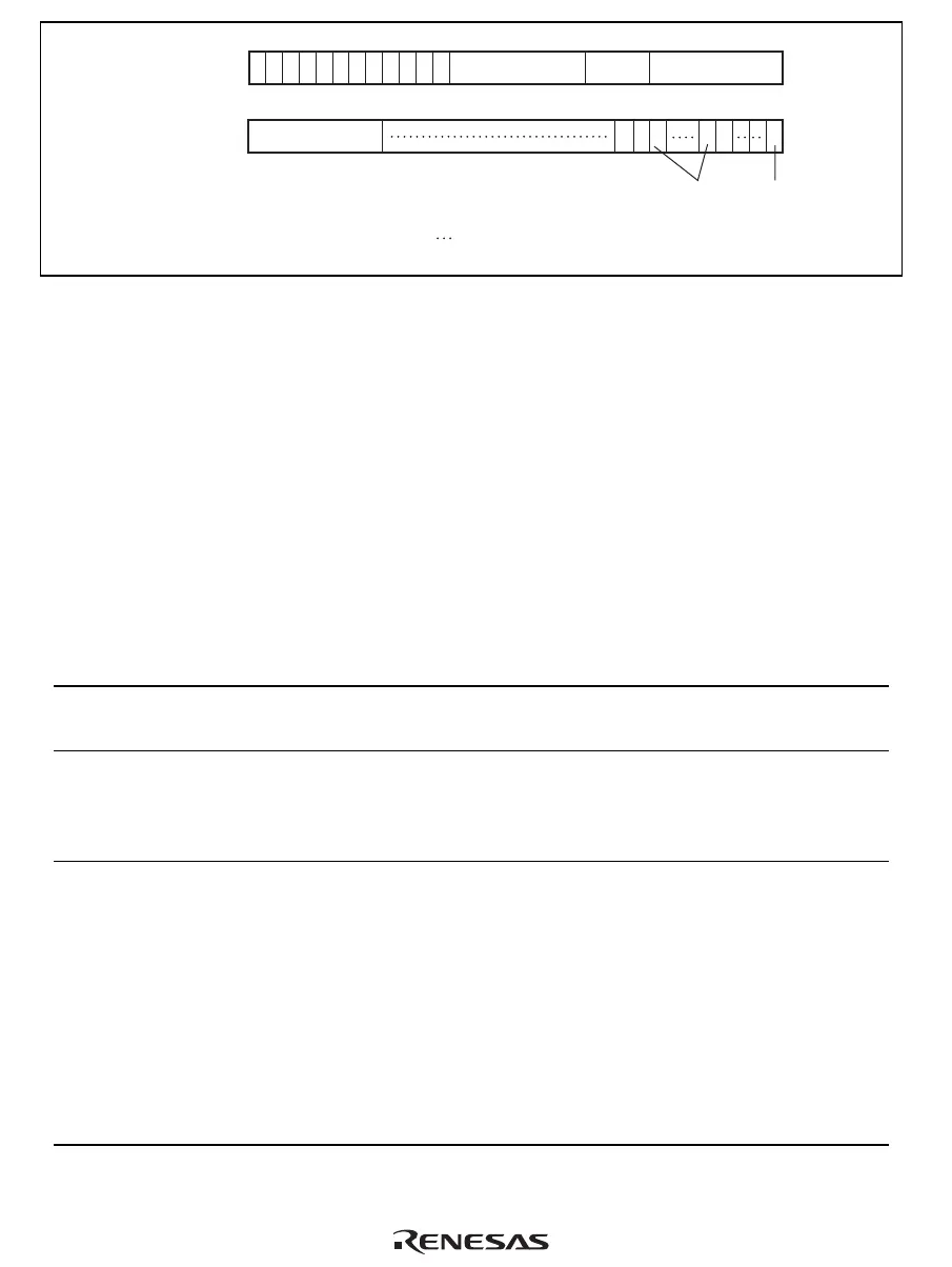
Address field
Data field
PPN:
V:
E:
SZ:
Physical page number
Validity bit
Entry
Page size bits
UB:
C:
WT:
:
Buffered write bit
Cacheability bit
Write-through bit
Reserved bits
(write value should be 0
and read value is undefined )
31 210
V
UB
10 9 8 74365
C
PPN
31 0
1111011
10001 E
2324
1920 8
712 11
SZ
WT
00000000 00000000
Figure 7.19 Memory-Mapped PMB Data Array
7.7.6 Notes on Using 32-Bit Address Extended Mode
When using 32-bit address extended mode, note that the items described in this section are
extended or changed as follows.
PASCR: The SE bit is added in bit 31 in the control register (PASCR). The bits 6 to 0 of the UB
in the PASCR are invalid (Note that the bit 7 of the UB is still valid). When writing to the P1 or
P2 area, the UB bit in the PMB controls whether a buffered write is performed or not. When the
MMU is enabled, the UB bit in the TLB controls writing to the P0, P3, or U0 area. When the
MMU is disabled, writing to the P0, P3, or U0 area is always performed as a buffered write.
Bit Bit Name
Initial
Value R/W Description
31 SE 0 R/W 0: 29-bit address mode
1: 32-bit address extended mode
30 to 8 All 0 R Reserved
For details on reading from or writing to these bits, see
description in General Precautions on Handling of
Product.
7 to 0 UB All 0 R/W Buffered Write Control for Each Area (64 Mbytes)
When writing is performed without using the cache or in
the cache write-through mode, these bits specify
whether the CPU waits for the end of writing for each
area.
0: The CPU does not wait for the end of writing
1: The CPU stalls and waits for the end of writing
UB[7]: Corresponding to the control register area
UB[6:0]: These bits are invalid in 32-bit address
extended mode.

 Loading...


