Rev. 1.50, 10/04, page 167 of 448
8.2.4 On-Chip Memory Control Register (RAMCR)
RAMCR controls the number of ways in the IC and OC.
RAMCR modifications must only be made by a program in the non-cacheable P2 area. After
RAMCR has been updated, execute one of the following three methods before an access
(including an instruction fetch) to the cacheable area or the L memory area is performed.
1. Execute a branch using the RTE instruction. In this case, the branch destination may be the
non-cacheable area or the L memory area.
2. Execute the ICBI instruction for any address (including non-cacheable area).
3. If the R2 bit in IRMCR is 0 (initial value) before updating RAMCR, the specific instruction
does not need to be executed. However, note that the CPU processing performance will be
lowered because the instruction fetch is performed again for the next instruction after RAMCR
has been updated.
Note that the method 3 may not be guaranteed in the future SuperH Series. Therefore, it is
recommended that the method 1 or 2 should be used for being compatible with the future SuperH
Series.
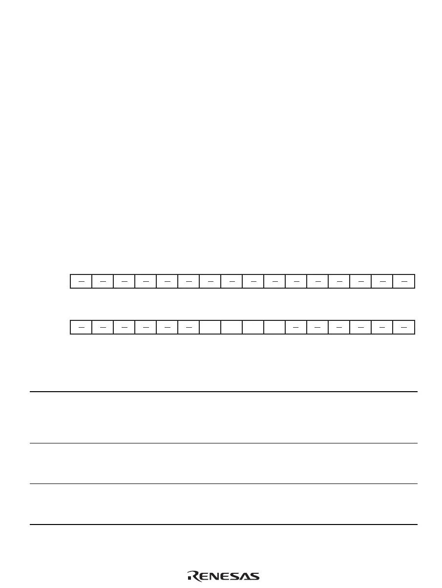
31 30 29 28 27 26 25 24 23 22 21 20 19 18 17 16
Bit:
Initial value:
RRRRRRRRRR
RMD RP IC2W OC2W
RRRRRR
0000000000000000
0000000000000000
R R R R R R R/W R/W R/W R/W R R R R R R
R/W:
Bit:
Initial value:
R/W:
15 14 13 12 11 10 9 8 7 6 5 4 3 2 1
0
Bit Bit Name
Initial
Value R/W Description
31 to 10 All 0 R Reserved
For details on reading from or writing to these bits, see
description in General Precautions on Handling of
Product.
9 RMD 0 R/W On-Chip Memory Access Mode Bit
For details, see section 9.4, L Memory Protective
Functions.
8 RP 0 R/W On-Chip Memory Protection Enable Bit
For details, see section 9.4, L Memory Protective
Functions.

 Loading...


