Rev. 1.50, 10/04, page 18 of 448
Bit Bit Name
Initial
Value R/W Description
17 to 12 Cause All 0 R/W
11 to 7 Enable (EN) All 0 R/W
6 to 2 Flag All 0 R/W
FPU Exception Cause Field
FPU Exception Enable Field
FPU Exception Flag Field
Each time an FPU operation instruction is executed, the
FPU exception cause field is cleared to 0. When an
FPU exception occurs, the bits corresponding to FPU
exception cause field and flag field are set to 1. The
FPU exception flag field remains set to 1 until it is
cleared to 0 by software.
For bit allocations of each field, see table 2.2.
1, 0 RM 01 R/W Rounding Mode
These bits select the rounding mode.
00: Round to Nearest
01: Round to Zero
10: Reserved
11: Reserved
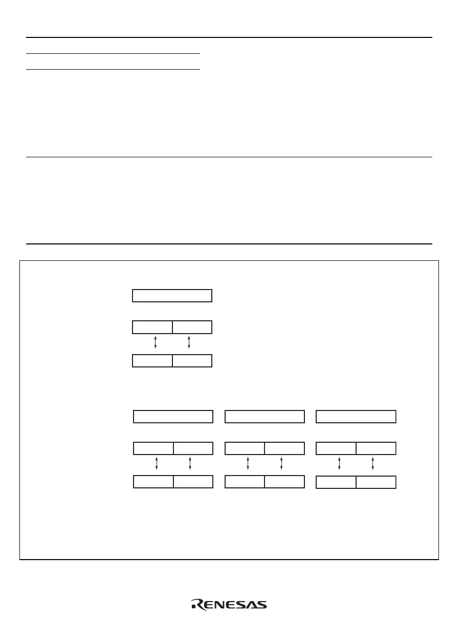
<Big endian>
DR (2i)
FR (2i) FR (2i+1)
8n+4 8n+78n 8n+3
63 0
63 32 31 0
Floating-point register
Memory area
63 0
<Little endian>
Floating-point register
Memory area
DR (2i)
FR (2i) FR (2i+1)
4n 4m4n+3 4m+3
63 0
63 32
31 0
DR (2i)
FR (2i+1)FR (2i)
8n+48n+78n+3 8n
63 0
63 32 31 0
(1) SZ = 0 (2) SZ = 1, PR = 0
63 0 63 0
DR (2i)
FR (2i+1)FR (2i)
8n8n+38n+7 8n+4
63 0
63 32
31 0
(3) SZ = 1, PR = 1
63 0
*
1,
*
2
*
2
Notes: 1. In the case of SZ = 0 and PR = 0, DR register can not be used.
2. The bit-location of DR register is used for double precision format when PR = 1.
(In the case of (2), it is used when PR is changed from 0 to 1.)
Figure 2.5 Relationship between SZ bit and Endian

 Loading...


