RFL 9300 RFL Electronics Inc.
September 5, 2007 xi (973) 334-3100
Figure 8-1. Single relay test setups ......................................................................................................................................... 4
Figure 8-2. Test connections simulating an internal A-G fault ............................................................................................. 12
Figure 8-3. Test connections simulating an internal A-B fault ............................................................................................. 15
Figure 8-4. Test connections simulating an internal three-phase fault.................................................................................. 16
Figure 8-5. Electrical connections between RFL 9300 and current transformers on protected line ..................................... 27
Figure 8-6. Correctly wired two-terminal system ................................................................................................................. 31
Figure 8-7. Phase inversion at remote 1 relay....................................................................................................................... 31
Figure 8-8. Phase inversion at local relay ............................................................................................................................. 32
Figure 8-9. Correctly wired three-terminal system ............................................................................................................... 33
Figure 8-10. Phase inversion at remote 2.............................................................................................................................. 34
Figure 8-11. Phase inversion at remote 1.............................................................................................................................. 35
Figure 8-12. Phase inversion at local station......................................................................................................................... 36
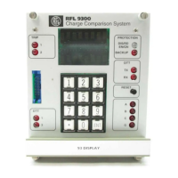
Figure 9-1. RFL 9300 display module for horizontal chassis ................................................................................................. 1
Figure 9-2. Controls and indicators for display controller board, used in RFL 9300 display module.................................... 3
Figure 9-3. Controls and indicators for oscillography board, used in RFL 93B DISPLAY module ...................................... 7
Figure 9-4. Component locator drawing for display controller board, used in RFL 9300 display module .......................... 12
Figure 9-5. Component locator drawing for oscillography board, used in RFL 9300 display module................................. 15
Figure 9-6. Component locator drawing for front panel assembly, used in RFL 9300 display module ............................... 17
Figure 9-7. Oscillography Board, part of RFL 9300 display module (Assembly No. 106330; Schematic No. D-106764-A)
Sheets 1 of 5 through 5 of 5 ........................................................................................................................................... 18
Figure 10-1. RFL 9300 supervisor controller module............................................................................................................. 1
Figure 10-2. Controls and indicators, RFL 9300 supervisor controller module ..................................................................... 2
Figure 10-3. Component locator drawing, supervisor controller modules for RFL 9300..................................................... 12
Figure 10-4. Supervisor Controller module for RFL 9300 Charge Comparison System(Assembly No. 106300; Schematic
No. D-106304-1-B) Sheets 1 of 2 and 2 of 2 ................................................................................................................ 13
Figure 11-1. RFL 93B ACT I/O Auxiliary Current Transformer I/O Module........................................................................ 1
Figure 11-2. Controls and indicators, RFL 93B ACT I/O Auxiliary Current Transformer I/O Module................................. 2
Figure 11-3. Block diagram, RFL 93B ACT I/O Auxiliary Current Transformer I/O Module .............................................. 3
Figure 11-4. Component locator drawing, RFL 93B ACT-5 5-Ampere Auxiliary Current Transformer I/O Module........... 6
Figure 11-5. RFL 93B ACT-5 5-Ampere Auxiliary Current Transformer I/O Module (Assembly No. 106345; Schematic
No. D-105814, Rev. C) .................................................................................................................................................... 7
Figure 12-1. RFL 9300 phase controller module .................................................................................................................... 1
Figure 12-2. Controls and indicators, RFL 9300 phase controller modules ........................................................................... 2
Figure 12-3. Component locator drawing, phase controller modules for RFL 9300 Charge Comparison System................. 7
Figure 12-4. Phase Controller modules for RFL 9300 Charge Comparison System (Assembly No. 106370; Schematic No.
D-103819, Rev. D) Sheets 1 of 2 an 2 of 2 ..................................................................................................................... 8
Figure 13-1. RFL 9300 communications controller module................................................................................................... 1
Figure 13-2. Controls and indicators, RFL 9300 communications controller module............................................................ 2
Figure 13-3. Block diagram, RFL 9300 communications controller module.......................................................................... 4
Figure 13-4. Transmitter timing diagram, RFL 9300 communications controller module ..................................................... 7
Figure 13-5. Receiver timing diagram, RFL 9300 communications controller module.......................................................... 8
Figure 13-6. Logic diagram for programmable logic device U24......................................................................................... 10
Figure 13-7. Component locator drawing, communications controller module for RFL 9300............................................. 13
Figure 13-8. Communications Controller modules for RFL 9300 Charge Comparison System (Assembly No. 106365;
Schematic No. D-103824, Rev. A) Sheets 1 of 2 and 2 and 2 ...................................................................................... 14
Figure 14-1. RFL 9300 modem module.................................................................................................................................. 1
Figure 14-2. Controls and indicators, RFL 9300 modem module........................................................................................... 2
Figure 14-3. Component locator drawing, modem module for RFL 9300 Charge Comparison System................................ 8
Figure 14-4. Modem module for RFL 9300 Charge Comparison System (Assembly No. 106355; Schematic No. D-
103829, Rev. B) ............................................................................................................................................................... 9