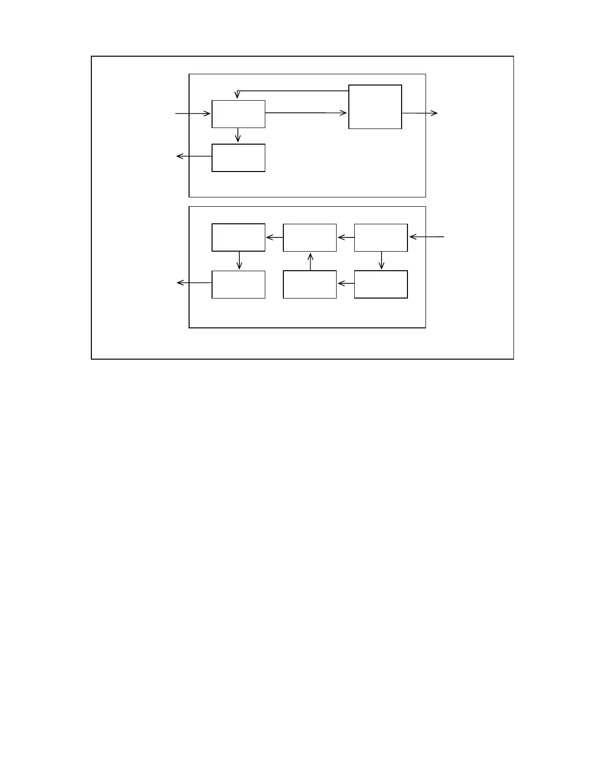
RX DATA TO
TRANSCEIVER
TX DATA FROM
TRANSCEIVER
TX ALM TO
TRANSCEIVER
LASER
EMITTER
LIGHT OUTPUT
TO FIBER OPTIC
CABLE
LIGHT INPUT
TO FIBER OPTIC
CABLE
DETECTOR
LIGHT LEVEL
DETECTOR
TRANS-
IMPEDANCE
AMPLIFIER
GAIN
CONTROL
AMPLIFIERS
THRESHOLD
DETECTOR
DETECTOR SECTION
EMITTER SECTION
FAILURE
DETECTOR
DRIVER
FEEDBAC
Figure 18-7. Block diagram, RFL 93 FT/FR 13SL (1300-nm Singlemode) and RFL 93 FT/FR 15SL (1550-nm Sin-
glemode)
Transmit Section
The fiber optic laser diode U2 is driven from a current source generated by Q1. A photodiode inside U2 senses
the light output of the laser diode and produces a current proportional to the output light level. This current pro-
duces a voltage across R12 and R13. The voltage level can be adjusted using R12. This voltage is then com-
pared to a reference voltage by U3, which performs as an integrating comparator. The output of U3 controls the
base of Q1 through R17 and one of the transistors in U1, which in turn will control the current through the laser
diode. This feedback loop will control the average output level of the laser diode, independent of temperature or
component variations.
The digital Tx data modulation signal is attenuated by R1 and R2, and coupled to the base of Q1 through C1
and one of the transistors in U1. This causes the laser diode current to vary from slightly above the laser
threshold current to a current that will produce the rated output power under a 50% modulation current condi-
tion.
A voltage proportional to the current in the laser diode is sensed at pin 4 of U1. This voltage is compared to a
reference voltage at pin 3 of U2, and will control Q1 to limit the maximum laser diode current to a safe level, if
necessary.
An alarm circuit is used to sense the proper operation of the laser control loop. Under normal operation, the volt-
ages at pins 2 and 3 of U3 should be nearly equal. These two voltages are buffered by the amplifiers in U4, and
applied to a window comparator formed by U5 and its associated circuitry. The comparison voltages are gener-
ated by resistors R5, R6, R7 and R8. The open collector outputs of the comparators in U5 are connected to pull
up resistor R4 and to the Tx alarm output on pin 2 of P2. The alarm output is active low.
RFL 9300 RFL Electronics Inc.
January 19, 2005 18 - 11 (973) 334-3100
 Loading...