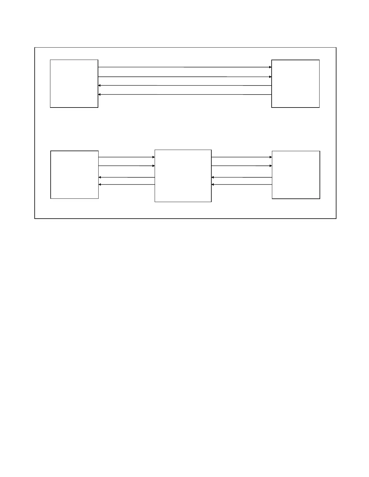
23.3.2 CLOCKING AND CONFIGURATIONS
Connection over two or four metallic wire pairs
Jumper J5 Set for “NORMAL” Jumper J5 Set for “NORMAL”
Connection through DCE equipment
Jumper J5 Set for “LOOP” Jumper J5 Set for “LOOP”
9300
Two Terminal,
Two Terminal +
Hot standby,
Three Terminal
93 G.703 interface
9300
Two Terminal, Two
Terminal + Hot
standby, Three
Terminal
93 G.703 interface
TX Clock and Data RX Clock and Data
RX Clock and Data TX Clock and Data
9300
Two Terminal,
Two Terminal +
Hot standby,
Three Terminal
93 G.703 interface
9300
Two Terminal, Two
Terminal + Hot
standby, Three
Terminal
93 G.703 interface
TX Clock and Data RX Clock and Data
RX Clock and Data
TX Clock and Data
DCE Equipment
Figure 23-3. Setting J5 for Normal or Loops Operation
23.3.3 PULSE INPUT/ OUTPUT CIRCUIT DESCRIPTION
The XRT6164 chip combined with transformers T1 and T2 forms a G.703 analog pulse to TTL pulse interface
with the Actel ( U1 ). The G.703 protocol is an AMI return to zero pulse. The TTL output from U2 separates the
positive and negative G.703 pulses and outputs a positive going pulse on S+R and S-R. This is a non-return to
zero signal that is suitable for digital logic. The specification for a G.703 pulse is one volt peak. Diodes at the
transformers (CR1- CR4) and (CR6 - CR9) limit transient peaks induced on the wires from coming into the mod-
ule. The diodes limit incoming signals to three forward diode drops or about 2.1 v. R2 is in series with the trans-
former and transistor collector outputs from the XRT6164 (TXD+ and TXD-). This allows adjustment of peak
levels into the 120 ohm termination presented by the external equipment. Transmitter calibration is accom-
plished by connecting a 120 ohm load between pins 2 and 9 of J1 and with the aid of an oscilloscope, set the
peak levels at 1 volt. R20 prevents overloading the transistors in U2 and damaging the chip.
23.3.4 RECEIVER PHASE LOCK LOOP CIRCUIT DESCRIPTION
The receiver phase lock loop consists of U1, U3, U4 and the surrounding discrete resistors and capacitors. U1
does very little in the phase locked loop. It only divides the output from U3 by 2 and outputs it on VCO_2. In ad-
dition, U1 combines positive and negative G.703 pulses into RX_P and RX_N with an OR gate and outputs the
resultant signal on PH_DET. This line contains all transitions and is the input to the receiver phase locked loop
circuit through J2. U3 combined with R5, R6, C2, R7 and C3 form a phase detector. The PH_DET line into U3 is
the reference. The VCO_2 line into U3 is the output from the phase detector, a 128 kHz signal. VCO_1 is a 256
kHz signal that is divided by two in the ACTEL and output on VCO_2. The G.703 RX pulses are at 128 kHz or
64 kHz depending on if the digital communication between 9300’s is sending a 0 or a 1. U4 is limited in output
frequency so that is must output a signal at or about 256 kHz even if the reference on PH_DET is 64 or 128
kHz. This keeps the phase locked loop from locking an octave away from the correct signal. Changes in the
clock rate from the receiver are slowly tracked and integrated. The resultant 128 kHz signal is again divided in
the Actel to create the receiver clock, a 64 kHz pulse.
RFL 9300 RFL Electronics Inc.
February 7, 2000 23 - 4 (973) 334-3100