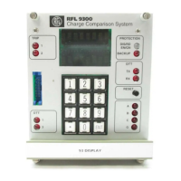
RFL 9300 RFL Electronics Inc.
May 1, 1998 16 - 3 (973) 334-3100
J3 J3 sets the polarity of the RECEIVE timing signal. Position A selects inverted polarity, and Posi-
tion B selects normal polarity. J3's setting will depend on the DCE being connected to the RFL
9300. Try to use the RFL 9300 with J3 in Position B; if the RECEIVE timing is not working prop-
erly, move J3 to Position A.
16.3 THEORY OF OPERATION
RFL 93 DD I/O operation is regulated by two control lines: STANDBY (at edge connector terminal P1-A18) and
TX CONTR (terminal P1-C18). When both control lines are low, the serial link paths go straight from the RFL 93B
CC module, through the motherboard, and on to rear-panel connector J1. For example, SEND timing comes in on
J1-5 and J1-23; if U4-1 is low, the timing pulses are passed to U4-7. The SEND timing signals can be inverted by
placing jumper J2 in Position A; Position B selects normal polarity. U4-7 then feeds a logic level to pin 15 of RS-
422 translator U1. The signals are again at RS-422 levels.
When the STANDBY line is high, the SEND timing enters the RFL 93 DD I/O as a logic level on edge connector
terminal P1-C15. Multiplexer U4 provides a path between U4-6 and U4-7. The source of the logic-level timing sig-
nal would be the RFL 93 DD I/O module plugged into rear panel Slot 2. When the RFL 93B CC module decides to
switch to Channel 2 in the hot standby configuration, it raises the STANDBY line.
The TX DATA path has a separate control line on edge connector terminal P1-C18, because the same data is
transmitted over both channels at all times in hot standby systems.
Jumpers J2 and J3 are both placed in Position B for normal operation. The RFL 93B CC module expects that the
received data is stable when the RECEIVE timing pulses are going from low to high (positive clock edge). If the
edges are not correct and the data is changing when the positive clock edge is received, J3 must be changed to
Position A. The RFL 93B CC module will produce stable TX DATA during the positive SEND timing clock edge;
J2 should be in Position B to avoid confusion.
J1-33 is the external /ALARM input. If not connected, pull-up resistor RZ1 defaults the /ALARM to the ALARM
OFF condition. The alarm is turned on by connecting J1-33 to J1-19 or J1-25 (signal ground).