Advanced control timer (TIM1) UM0306
170/519
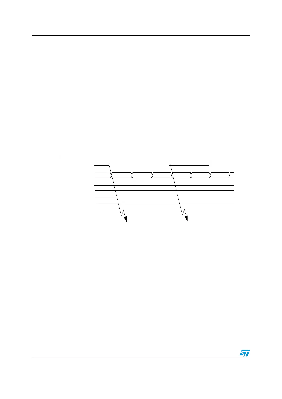
For example, you can measure the period (in TIM1_CCR1 register) and the duty cycle (in
TIM1_CCR2 register) of the PWM applied on TI1 using the following procedure (depending
on CK_INT frequency and prescaler value):
● Select the active input for TIM1_CCR1: write the CC1S bits to 01 in the TIM1_CCMR1
register (TI1 selected).
● Select the active polarity for TI1FP1 (used both for capture in TIM1_CCR1 and counter
clear): write the CC1P bit to ‘0’ (active on rising edge).
● Select the active input for TIM1_CCR2: write the CC2S bits to 10 in the TIM1_CCMR1
register (TI1 selected).
● Select the active polarity for TI1FP2 (used for capture in TIM1_CCR2): write the CC2P
bit to ‘1’ (active on falling edge).
● Select the valid trigger input: write the TS bits to 101 in the TIM1_SMCR register
(TI1FP1 selected).
● Configure the slave mode controller in reset mode: write the SMS bits to 100 in the
TIM1_SMCR register.
● Enable the captures: write the CC1E and CC2E bits to ‘1’ in the TIM1_CCER register.
Figure 54. PWM input mode timing.
12.4.8 Forced output mode
In output mode (CCxS bits = 00 in the TIM1_CCMRx register), each output compare signal
(OCxREF and then OCx/OCxN) can be forced to active or inactive level directly by software,
independently of any comparison between the output compare register and the counter.
To force an output compare signal (OCXREF/OCx) to its active level, you just need to write
101 in the OCxM bits in the corresponding TIM1_CCMRx register. Thus OCXREF is forced
high (OCxREF is always active high) and OCx get opposite value to CCxP polarity bit.
For example: CCxP=0 (OCx active high) => OCx is forced to high level.
The OCxREF signal can be forced low by writing the OCxM bits to 100 in the TIM1_CCMRx
register.
Anyway, the comparison between the TIM1_CCRx shadow register and the counter is still
performed and allows the flag to be set. Interrupt and DMA requests can be sent
accordingly. This is described in the Output Compare Mode section below.
TI1
TIM1_CNT
0000 0001 0002 0003 0004 00000004
TIM1_CCR1
TIM1_CCR2
0004
0002
IC1 Capture
period measurement
reset counter
IC2 Capture
pulse width measurement
 Loading...


