UM0306 Analog/digital converter (ADC)
463/519
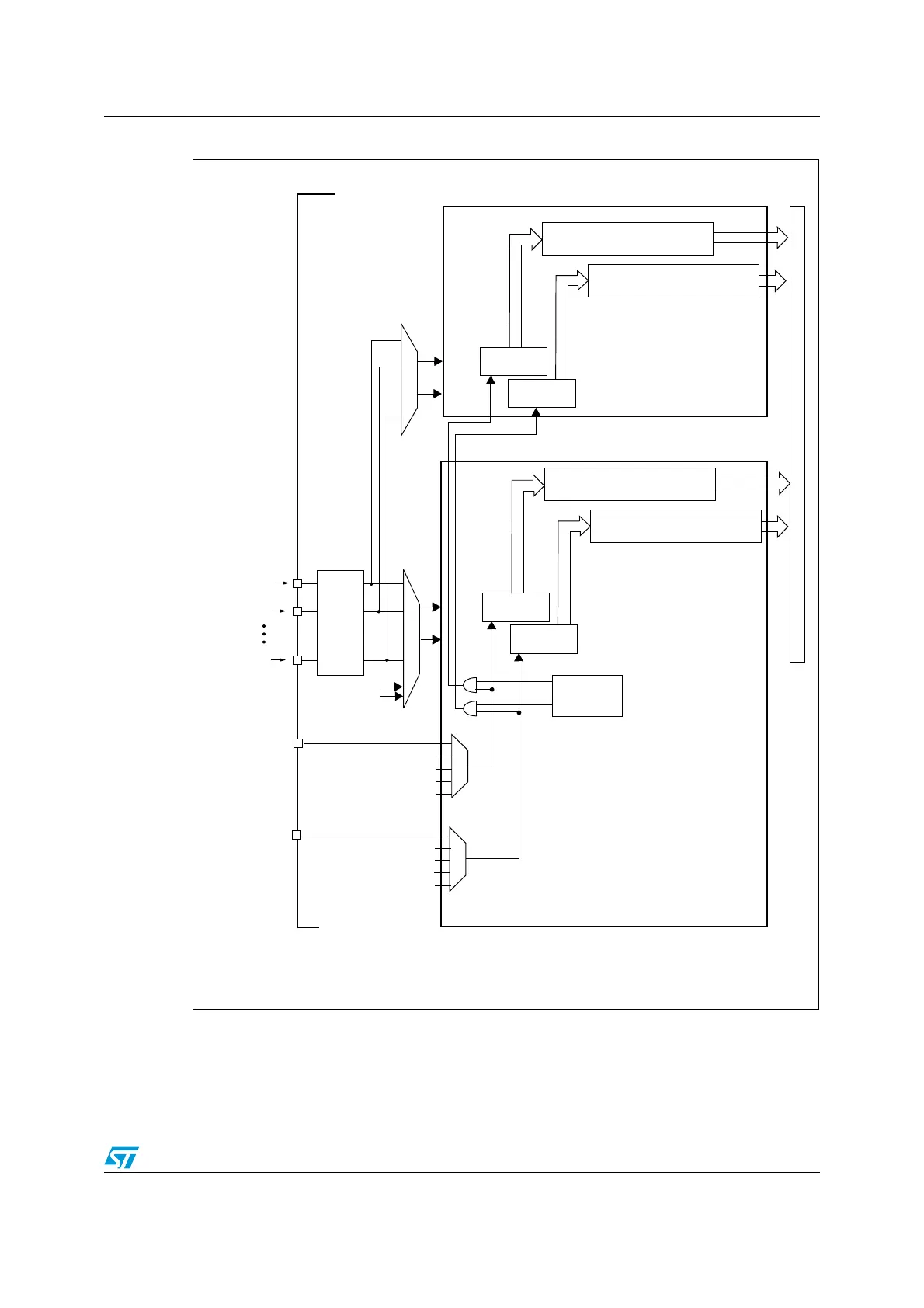
Figure 173. Dual ADC block diagram
ADC_IN0
ADC_IN1
ADC_IN15
GPIO
Ports
Address/data bus
EXTI_11
EXTI_15
INJECTED DATA REGISTERS
(4 x 16 bits)
REGULAR
CHANNELS
INJECTED
CHANNELS
ADC2 (SLAVE)
(12 bits)
INJECTED DATA REGISTERS
(4 x 16 bits)
REGULAR
CHANNELS
INJECTED
CHANNELS
ADC1 (MASTER)
DUAL MODE
internal triggers
Start trigger mux
(regular group)
(injected group)
Start trigger mux
CONTROL
Temp. sensor
V
REFINT
REGULAR DATA REGISTER
Note: External triggers are present on ADC2 but are not shown for the purposes of this diagram
(16 bits)
REGULAR DATA REGISTER
(16 bits)*
* In some dual ADC modes, the ADC1 data register (ADC1_DR) contains both ADC1 and ADC2 regular converted
data over the entire 32 bits.
 Loading...


