General purpose and alternate function I/O (GPIO and AFIO) UM0306
78/519
A set of Alternate Function I/O registers allow you to remap some alternate functions to
different pins. Refer to
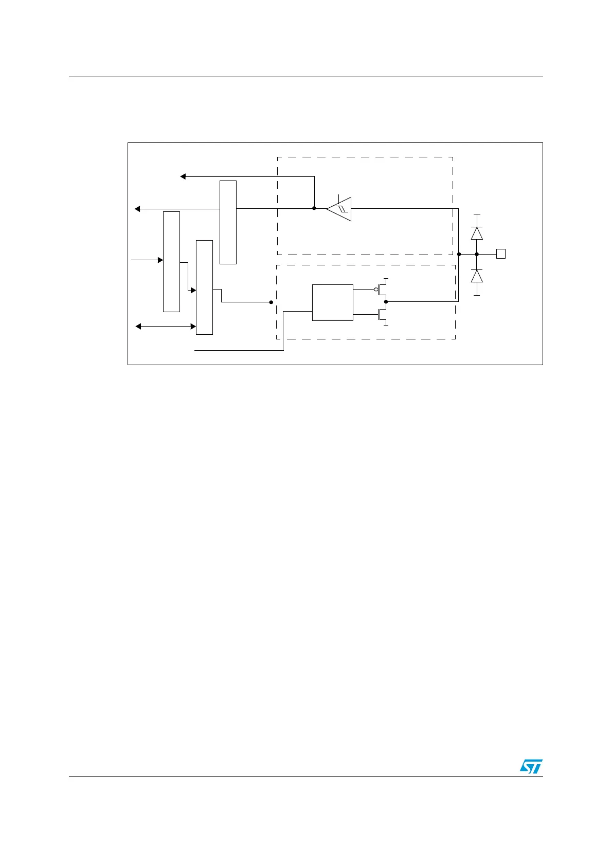
Figure 12. Alternate function configuration
5.1.10 Analog input configuration
When the I/O Port is programmed as Analog Input Configuration:
● The Output Buffer is disabled.
● The Schmitt Trigger Input is de-activated providing zero consumption for every analog
value of the I/O pin. The output of the Schmitt Trigger is forced to a constant value (0).
● The weak pull-up and pull-down resistors are disabled.
● Read access to the Input Data Register gets the value “0”.
The Figure 13 on page 79 shows the High impedance-Analog Input Configuration of the I/O
Port bit.
Alternate Function Output
Alternate Function Input
PUSH-PULL OR
OPEN-DRAIN
FROM ON-CHIP
PERIPHERAL
TO ON-CHIP
PERIPHERAL
OUTPUT
CONTROL
I/O PIN
VDD_IO
VSS
TTL SCHMITT
TRIGGER
VSS
VDD_IO
PROTECTION
DIODE
PROTECTION
DIODE
ON
INPUT DRIVER
OUTPUT DRIVER
P-MOS
N-MOS
INPUT DATA REGISTER
OUTPUT DATA REGISTER
READ/WRITE
READ
BIT SET/RESET REGISTERS
WRITE
 Loading...


