Advanced control timer (TIM1) UM0306
174/519
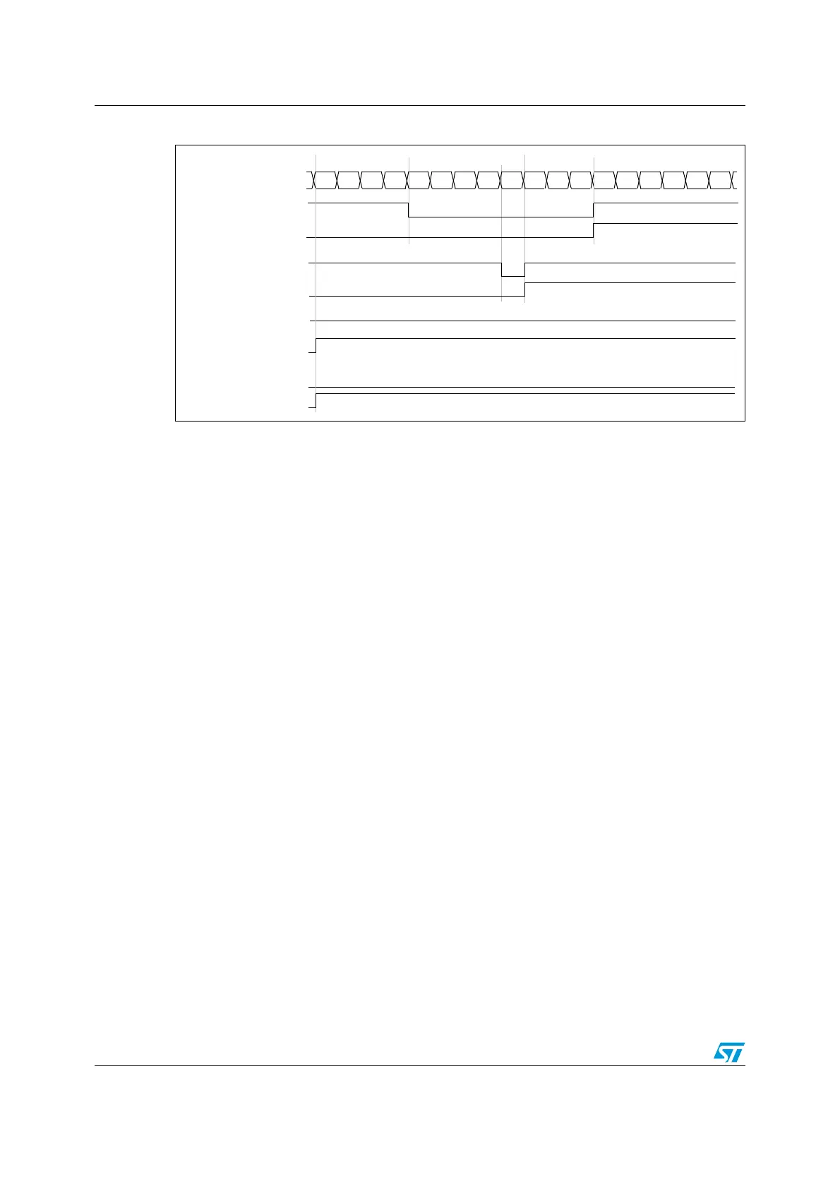
Figure 57. Center-aligned PWM waveforms (ARR=8)
Hints on using center-aligned mode:
● When starting in center-aligned mode, the current up-down configuration is used. It
means that the counter counts up or down depending on the value written in the DIR bit
in the TIM1_CR1 register. Moreover, the DIR and CMS bits must not be changed at the
same time by the software.
● Writing to the counter while running in center-aligned mode is not recommended as it
can lead to unexpected results. In particular:
– The direction is not updated if you write a value in the counter that is greater than
the auto-reload value (TIM1_CNT>TIM1_ARR). For example, if the counter was
counting up, it continues to count up.
– The direction is updated if you write 0 or write the TIM1_ARR value in the counter
but no Update Event UEV is generated.
● The safest way to use center-aligned mode is to generate an update by software
(setting the UG bit in the TIM1_EGR register) just before starting the counter and not to
write the counter while it is running.
12.4.11 Complementary outputs and dead-time insertion
The Advanced Control Timer TIM1 can output two complementary signals and manage the
switching-off and the switching-on instants of the outputs.
This time is generally known as dead-time and you have to adjust it depending on the
devices you have connected to the outputs and their characteristics (intrinsic delays of level-
shifters, delays due to power switches...)
You can select the polarity of the outputs (main output OCx or complementary OCxN)
independently for each output. This is done by writing to the CCxP and CCxNP bits in the
TIM1_CCER register.
The complementary signals OCx and OCxN are activated by a combination of several
control bits: the CCxE and CCxNE bits in the TIM1_CCER register and the MOE, OISx,
OISxN, OSSI and OSSR bits in the TIM1_BDTR and TIM1_CR2 registers. Refer to
Table 37: Output control bits for complementary OCx and OCxN channels with break feature
on page 211 for more details. In particular, the dead-time is activated when switching to the
IDLE state (MOE falling down to 0).
COUNTER REGISTER
‘1’
0
1234567876
‘0’
ocxref
CCxIF
ocxref
CCxIF
ocxref
CCxIF
ocxref
CCxIF
CCRx=4
CCRx=7
CCRx>=8
CCRx=0
5432101
 Loading...


