UM0306 Inter-integrated circuit (I2C) interface
337/519
Master receiver
Following the address transmission and after clearing ADDR, the I
2
C interface enters
Master Receiver mode. In this mode the interface receives bytes from the SDA line into the
DR register via the internal shift register. After each byte the interface generates in
sequence:
● An acknowledge pulse if the ACK bit is set
● The RxNE bit is set and an interrupt is generated if the ITEVFEN and ITBUFEN bits are
set (see Figure 138 Transfer sequencing EV7).
If the RxNE bit is set and the data in the DR register is not read before the end of the last
data reception, the BTF bit is set by hardware and the interface waits for a read in the DR
register.
Closing the communication
The master sends a NACK for the last byte received from the slave. After receiving this
NACK, the slave releases the control of the SCL and SDA lines. Then the master can send
a Stop/Re-Start condition.
● In order to generate the non-acknowledge pulse after the last received data byte, the
ACK bit must be cleared just after reading the second last data byte (after second last
RxNE event).
● In order to generate the Stop/Re-Start condition, software must set the STOP/START
bit just after reading the second last data byte (after the second last RxNE event).
After the Stop condition generation, the interface goes automatically back to slave mode
(M/SL bit cleared).
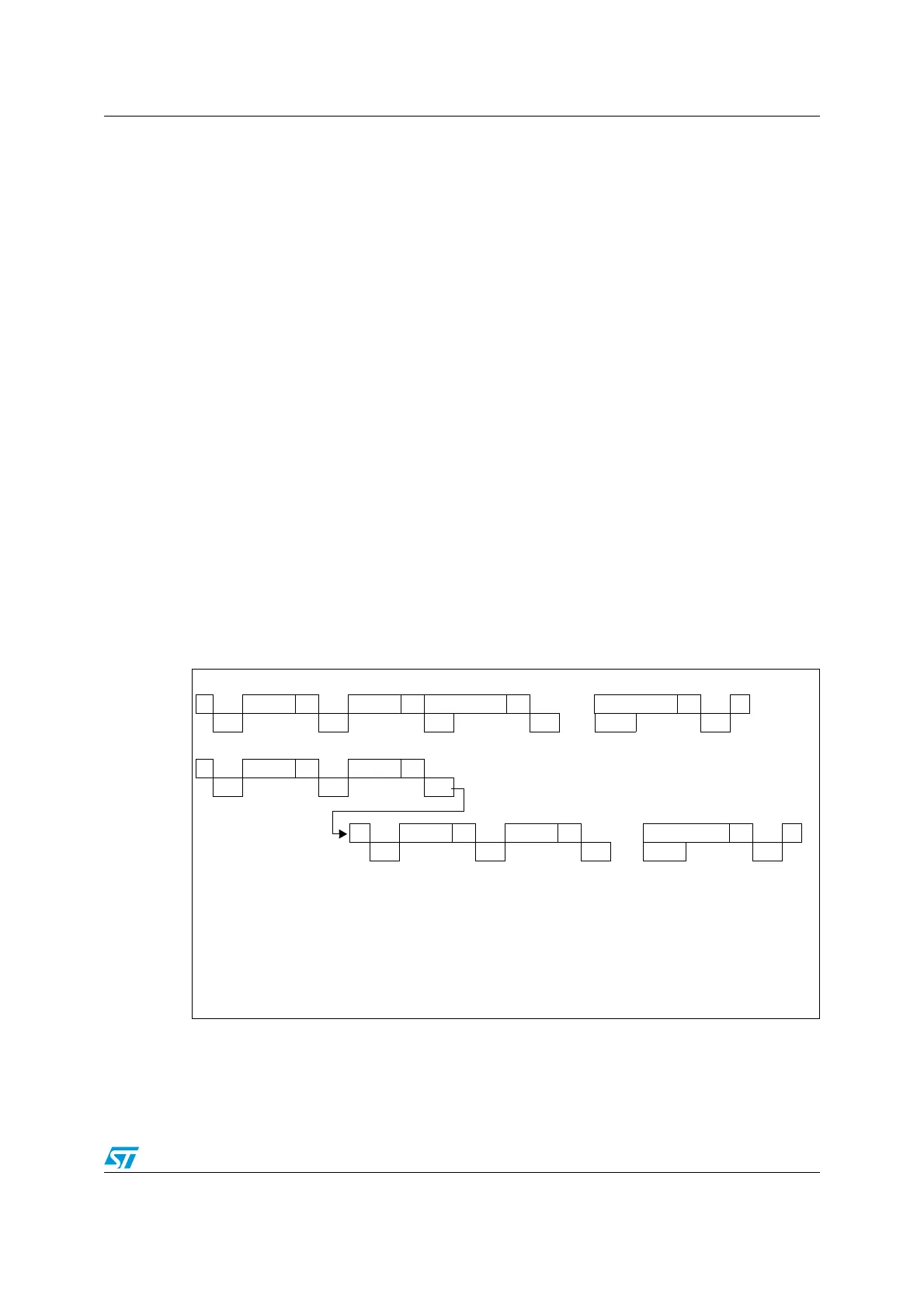
Figure 138. Transfer sequence diagram for master receiver
7-bit Master Receiver:
10-bit Master Receiver
Legend: S= Start, S
r
= Repeated Start, P= Stop, A= Acknowledge, NA= Non-acknowledge,
EVx= Event (with interrupt if ITEVFEN=1)
EV5: SB=1, cleared by reading SR1 register followed by writing DR register.
EV6: ADDR=1, cleared by reading SR1 register followed by reading SR2. In 10-bit master receiver mode, this se-
quence should be followed by writing CR2 with START = 1.
EV7: RxNE=1 cleared by reading DR register.
EV7_1: RxNE=1 cleared by reading DR register, program ACK=0 and STOP request
EV9: ADD10=1, cleared by reading SR1 register followed by writing DR register.
S Address A Data1 A Data2 A
.....
DataN NA P
EV5 EV6 EV7 EV7 EV7_1 EV7
S Header A Address A
EV5 EV9 EV6
S
r
Header A Data1 A
.....
DataN NA P
EV5 EV6 EV7 EV7_1 EV7
 Loading...


