Reset and clock control (RCC) UM0306
46/519
4.1.2 Power Reset
A power Reset is generated when one of the following events occurs:
1. Power On/Power down Reset (POR/PDR Reset)
2. When exiting STANDBY mode
A power Reset sets all registers to their reset values except the Backup domain (see
Figure 3)
These sources act on the RESET
pin and it is always kept low during the delay phase. The
RESET service routine vector is fixed at addresses
0x0000_0000-0x0000_0004 in the memory
map.
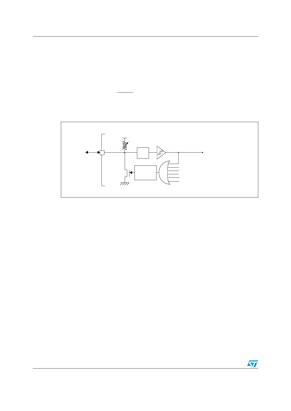
Figure 6. Reset circuit
The Backup domain has two specific resets that affect only the Backup domain (see
Figure 3)
4.1.3 Backup domain Reset
A backup domain Reset is generated when one of the following events occurs:
1. Software Reset, triggered by setting the BDRST bit in the Backup domain control
register (RCC_BDCR).
2. V
DD
or V
BAT
power on, if both supplies have previously been powered off.
4.2 Clocks
Three different clock sources can be used to drive the system clock (SYSCLK):
● HSI oscillator clock
● HSE oscillator clock
● PLL clock
The devices have the following two secondary clock sources:
● 32 kHz Low Speed Internal RC (LSI RC) which drives the Independent Watchdog and
optionally the RTC used for Auto Wake-up from STOP/STANDBY mode.
● 32.768 kHz Low Speed External crystal (LSE crystal) which optionally drives the Real-
Time Clock (RTCCLK)
NRST
R
ON
V
DD
WWDG Reset
IWDG Reset
PULSE
GENERATOR
POR/PDR Reset
EXTERNAL
RESET
(min 20µs)
SYSTEM NRESET
Filter
Software Reset
Low-power management Reset
 Loading...


