UM0306 Advanced control timer (TIM1)
211/519
Note: The state of the external I/O pins connected to the complementary OCx and
OCxN channels depends on the OCx and OCxN channel state and the GPIO and
AFIO registers.
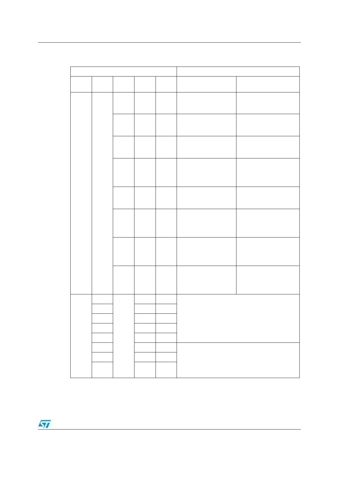
Table 37. Output control bits for complementary OCx and OCxN channels with
break feature
Control bits Output states
MOE
bit
OSSI
bit
OSSR
bit
CCxE
bit
CCxNE
bit
OCx Output State OCxN Output State
1X
000
Output Disabled (not
driven by the timer)
OCx=CCxP, OCx_EN=0
Output Disabled (not
driven by the timer)
OCxN=CCxNP, OCxN_EN=0
001
Output Disabled (not
driven by the timer)
OCx=CCxP, OCx_EN=0
OCxREF + Polarity
OCxN=OCxREF xor CCxNP,
OCxN_EN=1
010
OCxREF + Polarity
OCx=OCxREF xor CCxP,
OCx_EN=1
Output Disabled (not
driven by the timer)
OCxN=CCxNP, OCxN_EN=0
011
OCREF + Polarity +
dead-time
OCx_EN=1
Complementary to
OCREF (not OCREF) +
Polarity + dead-time
OCxN_EN=1
100
Output Disabled (not
driven by the timer)
OCx=CCxP, OCx_EN=0
Output Disabled (not
driven by the timer)
OCxN=CCxNP, OCxN_EN=0
101
Off-State (output
enabled with inactive
state)
OCx=CCxP, OCx_EN=1
OCxREF + Polarity
OCxN=OCxREF xor CCxNP,
OCxN_EN=1
110
OCxREF + Polarity
OCx=OCxREF xor CCxP,
OCx_EN=1
Off-State (output
enabled with inactive
state)
OCxN=CCxNP, OCxN_EN=1
111
OCREF + Polarity +
dead-time
OCx_EN=1
Complementary to
OCREF (not OCREF) +
Polarity + dead-time
OCxN_EN=1
0
0
X
00
Output Disabled (not driven by the timer)
Asynchronously: OCx=CCxP, OCx_EN=0, OCxN=CCxNP,
OCxN_EN=0
Then if the clock is present: OCx=OISx and OCxN=OISxN after a
dead-time, assuming that OISx and OISxN don’t correspond to
OCX and OCxN both to active state.
001
010
011
100
1 0 1 Off-State (output enabled with inactive state)
Asynchronously: OCx=CCxP, OCx_EN=1, OCxN=CCxNP,
OCxN_EN=1
Then if the clock is present: OCx=OISx and OCxN=OISxN after a
dead-time, assuming that OISx and OISxN don’t correspond to
OCX and OCxN both to active state
110
111
 Loading...


