Reset and clock control (RCC) UM0306
72/519
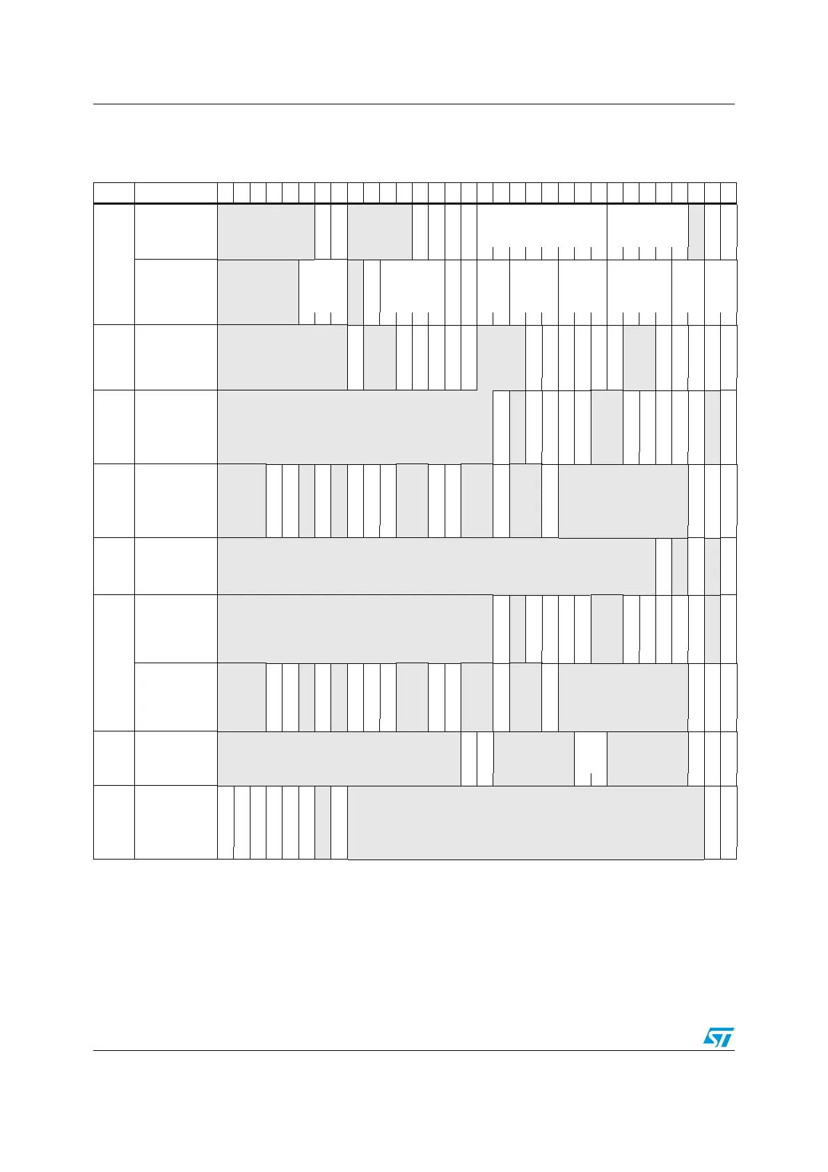
4.4 RCC register map
Refer to Table 1 on page 27 for the register boundary addresses.
Table 10.
RCC - register map and reset values
Offset Register
31
30
29
28
27
26
25
24
23
22
21
20
19
18
17
16
15
14
13
12
11
10
9
8
7
6
5
4
3
2
1
0
000h
RCC_CR
Reserved
PLL RDY
PLL ON
Reserved
CSSON
HSEBYP
HSERDY
HSEON
HSICAL[7:0] HSITRIM[4:0]
Reserved
HDIRDY
HDION
Reset Value 00 00000000000010000 11
004h
RCC_CFGR
Reserved
MCO [2:0]
Reserved
USBPRE
PLLMUL[3:0]
PLLXTPRE
PLLSRC
ADC
PRE
[1:0]
PPRE2
[2:0]
PPRE1
[2:0]
HPRE[3:0]
SWS
[1:0]
SW
[1:0]
Reset Value 000 00000000000000000000000
008h
RCC_CIR
Reserved
CSSC
Reserved
PLLRDYC
HSERDYC
HSIRDYC
LSERDYC
LSIRDYC
Reserved
PLLRDYIE
HSERDYIE
HSIRDYIE
LSERDYIE
LSIRDYIE
CSSF
Reserved
PLLRDYF
HSERDYF
HSIRDYF
LSERDYF
LSIRDYF
Reset Value 0 00000 000000 00000
00Ch
RCC_APB2RSTR
Reserved
USART1RST
Reserved
SPI1RST
TIM1RST
ADC2RST
ADC1RST
Reserved
IOPERST
IOPDRST
IOPCRST
IOPBRST
IOPARST
Reserved
AFIORST
Reset Value 0 0000 00000 0
010h
RCC_APB1RSTR
Reserved
PWRRST
BKPRST
Reserved
CANRST
Reserved
USBRST
I2C2RST
I2C1RST
Reserved
USART3RST
USART2RST
Reserved
SPI2RST
Reserved
WWDGRST
Reserved
TMI3RST
TM2RST
TMI1RST
Reset Value 00 0 000 00 0 0 000
014h
RCC_AHBENR
Reserved
FLITFEN
Reserved
SRAMEN
Reserved
DMAEN
Reset Value 1 1 0
018h
RCC_APB2ENR
Reserved
USART1EN
Reserved
SPI1EN
TIM1EN
ADC2EN
ADC1EN
Reserved
IOPEEN
IOPDEN
IOPCEN
IOPBEN
IOPAEN
Reserved
AFIOEN
Reset Value 0 0000 00000 0
01Ch
RCC_APB1ENR
Reserved
PWREN
BKPEN
Reserved
CANEN
Reserved
USBEN
I2C2EN
I2C1EN
Reserved
USART3EN
USART2EN
Reserved
SPI2EN
Reserved
WWDGEN
Reserved
TMI3EN
TM2EN
TMI1EN
Reset Value 00 0 000 00 0 0 000
020h
RCC_BDCR
Reserved
BDRST
RTCEN
Reserved
RTC
SEL
[1:0]
Reserved
LSEBYP
LSERDY
LSEON
Reset Value 0 0 0 0 0 0 0
024h
RCC_CSR
LPWRSTF
WWDGRSTF
IWDGRSTF
SFTRSTF
PORRSTF
PINRSTF
Reserved
RMVF
Reserved
LSIRDY
LSION
Reset Value 000011 0 00
 Loading...


