UM0306 Serial peripheral interface (SPI)
361/519
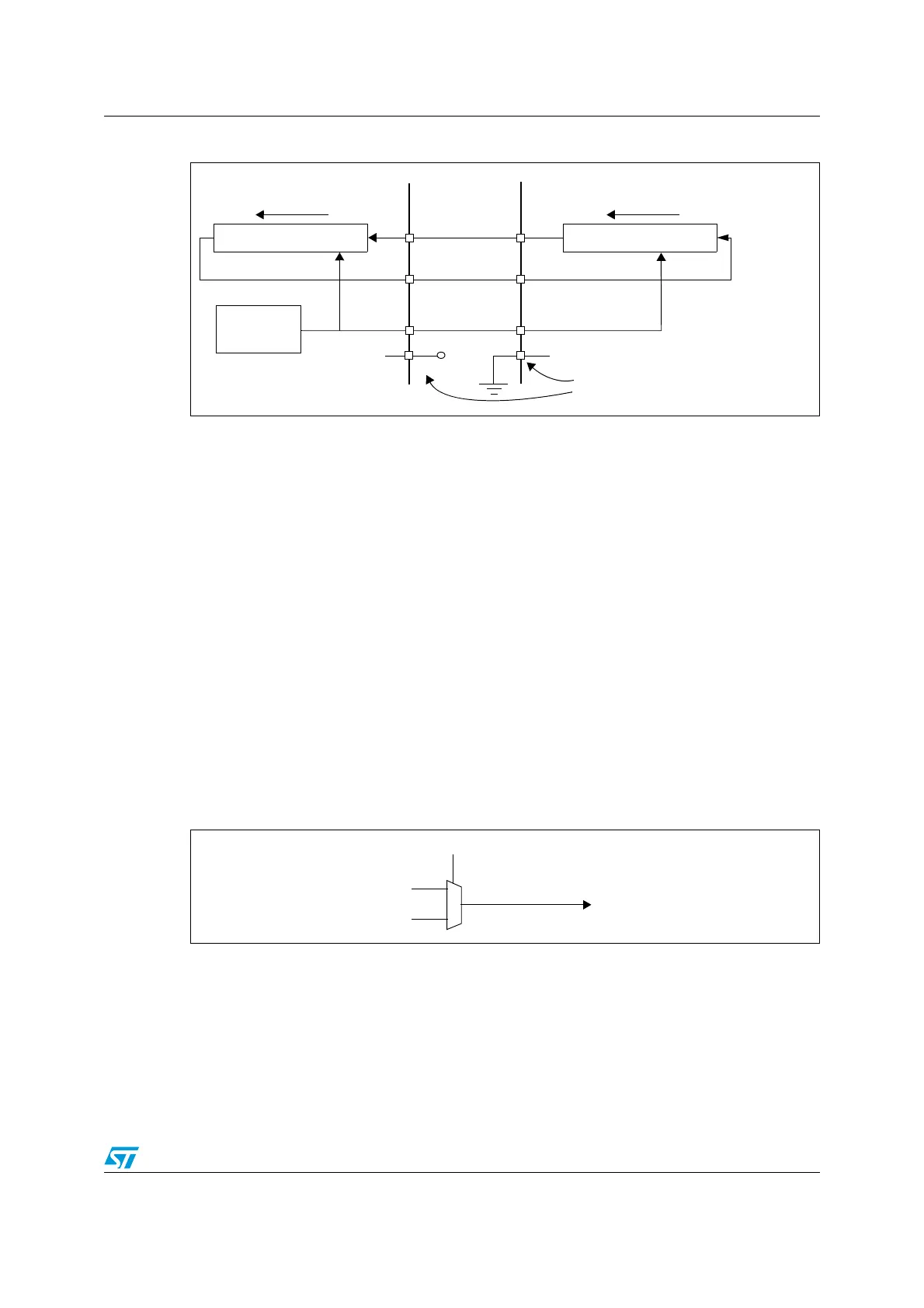
Figure 141. Single master/ single slave application
The MOSI pins are connected together and the MISO pins are connected together. In this
way data is transferred serially between master and slave (most significant bit first).
The communication is always initiated by the master. When the master device transmits
data to a slave device via MOSI pin, the slave device responds the MISO pin. This implies
full duplex communication with both data out and data in synchronized with the same clock
signal (which is provided by the master device via the SCK pin).
Slave select (NSS) pin management
The NSS pin can be used for both input (in hardware mode) and output. SS output is
enabled or disabled through the SSOE bit in the SPI_CR2 register. Multi-master
configurations are only possible when SS output is disabled. The NSS pin is driven low
when used as an output (SSOE bit) and the SPI is in master mode configuration. Thus all
NSS pins in SPI devices become slaves when they are configured in NSS mode.
As an alternative to using the NSS pin to control the Slave Select signal (NSS pin), the
application can choose to manage the Slave Select signal by software. This is configured by
the SSM bit in the SPI_CR1 register (see Figure 142). In software management, the
external NSS pin is free for other application uses and the internal NSS signal level is driven
by writing to the SSI bit in the SPI_CR1 register.
Figure 142. Hardware/software slave select management
Clock phase and clock polarity
Four possible timing relationships may be chosen by software, using the CPOL and CPHA
bits in the SPI_CR1 register. The CPOL (clock polarity) bit controls the steady state value of
the clock when no data is being transferred. This bit affects both master and slave modes. If
CPOL is reset, SCK pin has a low level idle state. If CPOL is set, SCK pin has a high level
idle state.
8-BIT SHIFT REGISTER
SPI
CLOCK
GENERATOR
8-BIT SHIFT REGISTER
MISO
MOSI
MOSI
MISO
SCK
SCK
SLAVE
MASTER
NSS
NSS
V
DD
MSBit LSBit MSBit LSBit
Not used if NSS is managed
by software
Note: Here, the NSS pin is configured as input
1
0
NSS Internal
SSM bit
SSI bit
NSS external pin
 Loading...


