Advanced control timer (TIM1) UM0306
172/519
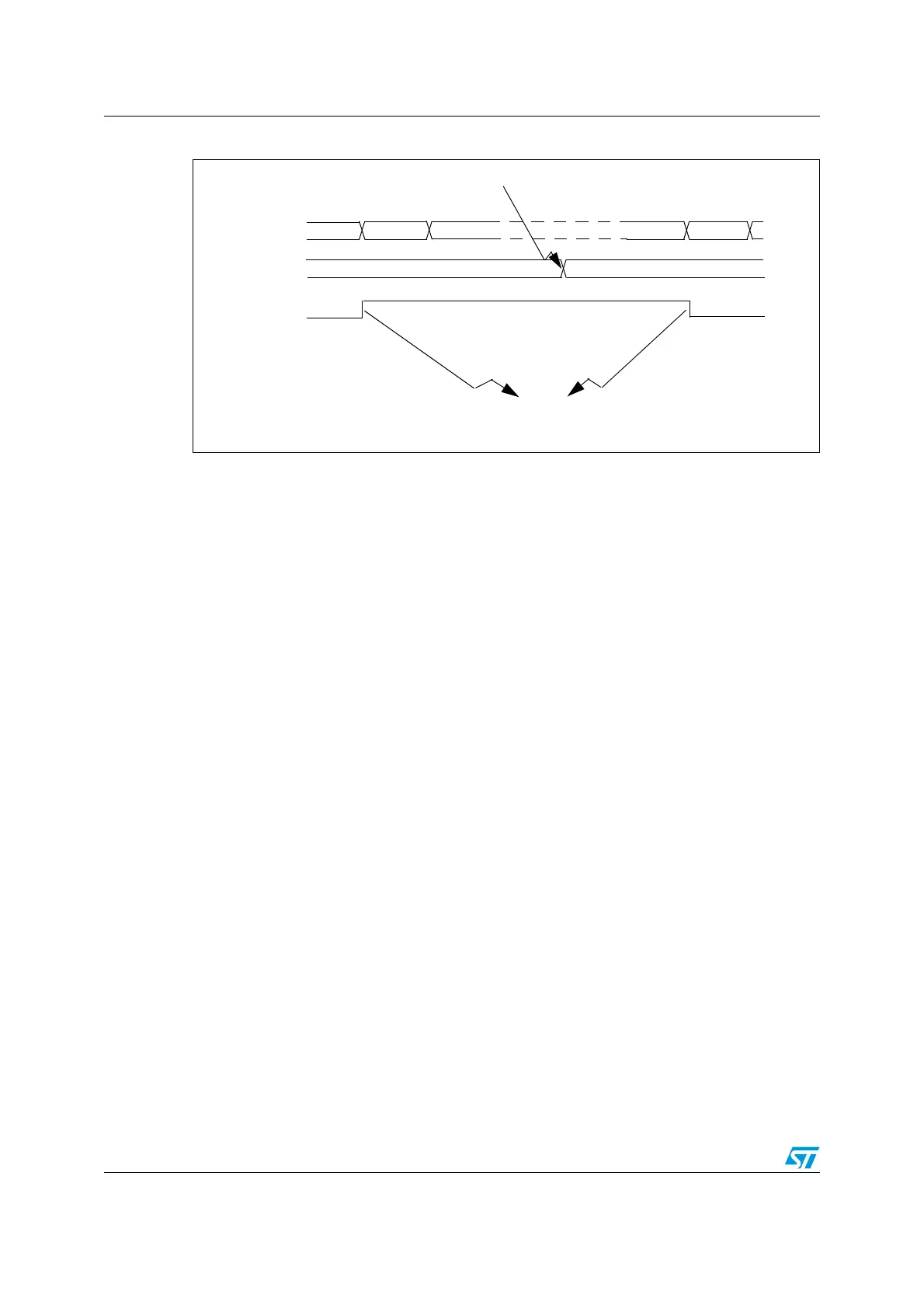
Figure 55. Output compare mode, toggle on OC1.
12.4.10 PWM mode
Pulse Width Modulation mode allows you to generate a signal with a frequency determined
by the value of the TIM1_ARR register and a duty cycle determined by the value of the
TIM1_CCRx register.
The PWM mode can be selected independently on each channel (one PWM per OCx
output) by writing ‘110’ (PWM mode 1) or ‘111’ (PWM mode 2) in the OCxM bits in the
TIM1_CCMRx register. You must enable the corresponding preload register by setting the
OCxPE bit in the TIM1_CCMRx register, and eventually the auto-reload preload register (in
up-counting or center-aligned modes) by setting the ARPE bit in the TIM1_CR1 register.
As the preload registers are transferred to the shadow registers only when an update event
occurs, before starting the counter, you have to initialize all the registers by setting the UG
bit in the TIM1_EGR register.
OCx polarity is software programmable using the CCxP bit in the TIM1_CCER register. It
can be programmed as active high or active low. OCx output is enabled by the CCxE bit in
the TIM1_CCER register when the break feature is not implemented, else by a combination
of CCxE, CCxNE, MOE, OSSI and OSSR bits (TIM1_CCER and TIM1_BDTR registers).
Refer to the TIM1_CCERx register description for more details.
In PWM mode (1 or 2), TIM1_CNT and TIM1_CCRx are always compared to determine
whether TIM1_CCRx≤TIM1_CNT or TIM1_CNT≤TIM1_CCRx (depending on the direction
of the counter).
The timer is able to generate PWM in edge-aligned mode or center-aligned mode
depending on the CMS bits in the TIM1_CR1 register.
PWM edge-aligned mode
Up-counting configuration
Up-counting is active when the DIR bit in the TIM1_CR1 register is low. Refer to the Up-
counting mode on page 154.
In the following example, we consider PWM mode 1. The reference PWM signal OCxREF is
high as long as TIM1_CNT <TIM1_CCRx else it becomes low. If the compare value in
TIM1_CCRx is greater than the auto-reload value (in TIM1_ARR) then OCxREF is held at
oc1ref=OC1
TIM1_CNT
B200 B201
0039
TIM1_CCR1
003A
Write B201h in the OC1R register
Match detected on OCR1
Interrupt generated if enabled
003B
B201
003A
 Loading...


