UM0306 General purpose and alternate function I/O (GPIO and AFIO)
77/519
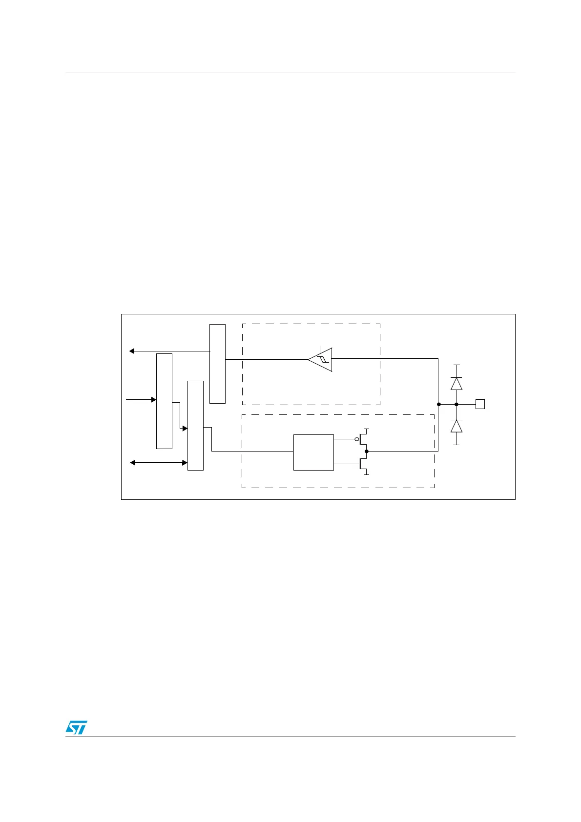
5.1.8 Output configuration
When the I/O Port is programmed as Output:
● The Output Buffer is enabled:
– Open Drain Mode: A “0” in the Output register activates the N-MOS while a “1” in
the Output register leaves the port in Hi-Z. (the P-MOS is never activated)
– Push-Pull Mode: A “0” in the Output register activates the N-MOS while a “1” in the
Output register activates the P-MOS.
● The Schmitt Trigger Input is activated.
● The weak pull-up and pull-down resistors are disabled.
● The data present on the I/O pin is sampled into the Input Data Register every APB2
clock cycle
● A read access to the Input Data Register gets the I/O state in open drain mode
● A read access to the Output Data register gets the last written value in Push-Pull mode
The Figure 11 on page 77 shows the Output configuration of the I/O Port bit.
Figure 11. Output configuration
5.1.9 Alternate function configuration
When the I/O Port is programmed as Alternate Function:
● The Output Buffer is turned on in Open Drain or Push-Pull configuration
● The Output Buffer is driven by the signal coming from the peripheral (alternate function
out)
● The Schmitt Trigger Input is activated
● The weak pull-up and pull-down resistors are disabled.
● The data present on the I/O pin is sampled into the Input Data Register every APB2
clock cycle
● A read access to the Input Data Register gets the I/O state in open drain mode
● A read access to the Output Data register gets the last written value in Push-Pull mode
The Figure 12 on page 78 shows the Alternate Function Configuration of the I/O Port bit.
Also, refer to Section 5.4: AFIO register description on page 91 for further information.
PUSH-PULL OR
OPEN-DRAIN
OUTPUT
CONTROL
I/O PIN
V
DD_IO
V
SS
TTL SCHMITT
TRIGGER
V
SS
V
DD_IO
PROTECTION
DIODE
PROTECTION
DIODE
ON
INPUT DRIVER
OUTPUT DRIVER
P-MOS
N-MOS
INPUT DATA REGISTER
OUTPUT DATA REGISTER
READ/WRITE
READ
BIT SET/RESET REGISTERS
WRITE
 Loading...


