Inter-integrated circuit (I2C) interface UM0306
332/519
Slave transmitter
Following the address reception and after clearing ADDR, the slave sends bytes from the
DR register to the SDA line via the internal shift register.
The slave stretches SCL low until ADDR is cleared and DR filled with the data to be sent
(see Figure 135 Transfer sequencing EV1 EV3).
When the acknowledge pulse is received:
● The TxE bit is set by hardware with an interrupt if the ITEVFEN and the ITBUFEN bits
are set.
If TxE is set and a data was not written in the DR register before the end of the last data
transmission, the BTF bit is set and the interface waits for a write in the DR register,
stretching SCL low.
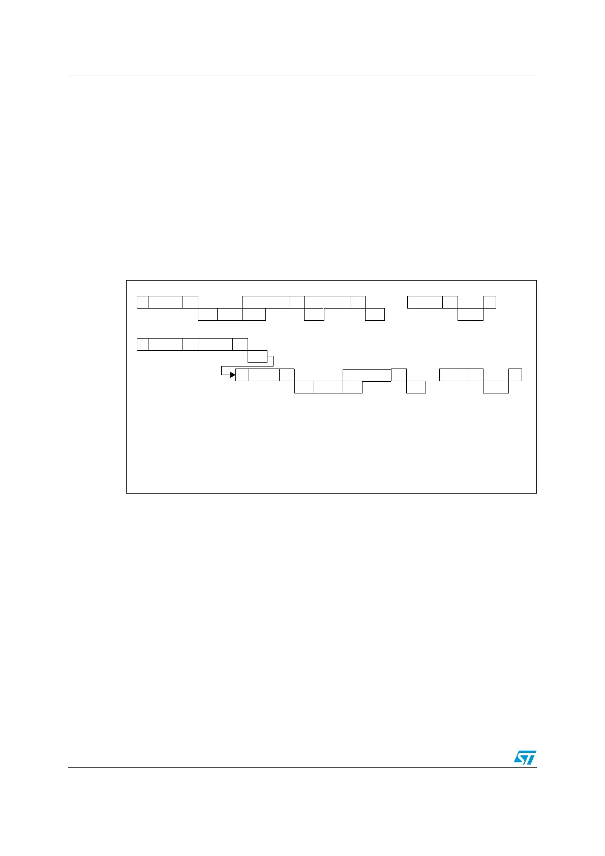
Figure 135. Transfer sequence diagram for slave transmitter
7-bit slave transmitter:
10-bit slave transmitter
Legend: S= Start, S
r
= Repeated Start, P= Stop, A= Acknowledge, NA= Non-acknowledge,
EVx= Event (with interrupt if ITEVFEN=1)
EV1: ADDR=1, cleared by reading SR1 followed by reading SR2
EV3-1: TxE=1, shift register empty.
EV3: TxE=1, cleared by writing DR; shift register not empty
EV3-2: AF=1; AF is cleared by writing ‘0’ in AF bit of SR1 register.
S Address A Data1 A Data2 A
.....
DataN NA P
EV1 EV3-1 EV3 EV3 EV3 EV3-2
S Header A Address A
EV1
S
r
Header A Data1 A
....
.
DataN NA P
EV1 EV3_1 EV3 EV3 EV3-2
 Loading...


