General purpose and alternate function I/O (GPIO and AFIO) UM0306
76/519
5.1.5 Software remapping of I/O alternate functions
To optimize the number of peripheral I/O functions for different device packages, it is
possible to remap some alternate functions to some other pins. This is achieved by
software, by programming the corresponding registers (refer to AFIO register description on
page 91. In that case, the alternate functions are no longer mapped to their original
assignations.
5.1.6 GPIO locking mechanism
The locking mechanism allows the IO configuration to be frozen. When the LOCK sequence
has been applied on a port bit, it is no longer possible to modify the value of the port bit until
the next reset.
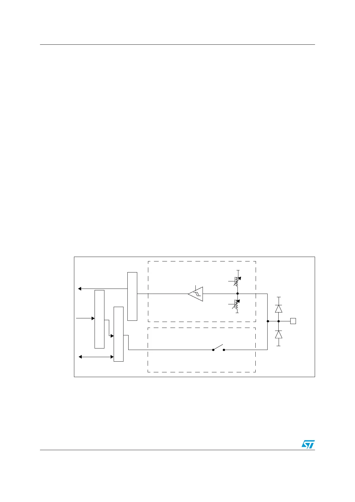
5.1.7 Input configuration
When the I/O Port is programmed as Input:
● The Output Buffer is disabled
● The Schmitt Trigger Input is activated
● The weak pull-up and pull-down resistors are activated or not depending on input
configuration (pull-up, pull-down or floating):
● The data present on the I/O pin is sampled into the Input Data Register every APB2
clock cycle
● A read access to the Input Data Register obtains the I/O State.
The Figure 10 on page 76 shows the Input Configuration of the I/O Port bit.
Figure 10. Input floating/pull up/pull down configurations
ON/OFF
PULL
PULL
ON/OFF
I/O PIN
V
DD_IO
V
SS
TTL SCHMITT
TRIGGER
V
SS
V
DD_IO
PROTECTION
DIODE
PROTECTION
DIODE
ON
INPUT DRIVER
OUTPUT DRIVER
DOWN
UP
INPUT DATA REGISTER
OUTPUT DATA REGISTER
READ/WRITE
READ
BIT SET/RESET REGISTERS
WRITE
 Loading...


