Reset and clock control (RCC) UM0306
54/519
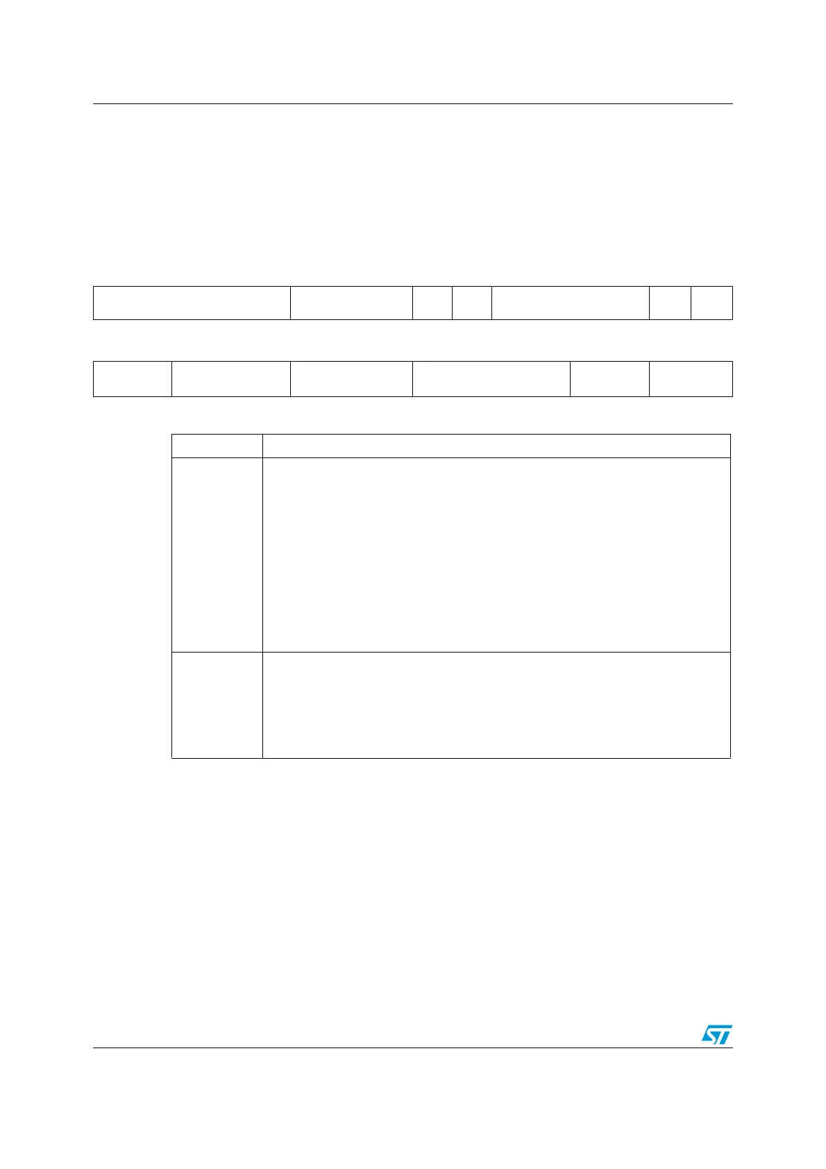
4.3.2 Clock configuration register (RCC_CFGR)
Address offset: 04h
Reset value: 0000 0000h
Access: 0 <= wait state <= 2, word, half-word and byte access
1 or 2 wait states inserted only if the access occurs during clock source switch.
31 30 29 28 27 26 25 24 23 22 21 20 19 18 17 16
Reserved MCO[2:0] Res.
USB
PRE
PLLMUL[3:0]
PLL
XTPRE
PLL
SRC
rw rw rw rw rw rw rw rw rw
1514131211109 87654321 0
ADC PRE[1:0] PPRE2[2:0] PPRE1[2:0] HPRE[3:0] SWS[1:0] SW[1:0]
rw rw rw rw rw rw rw rw rw rw rw rw r r rw rw
Bits 31:26 Reserved, always read as 0.
Bits 26:24
MCO Microcontroller Clock Output
Set and reset by software.
0xx: No clock
100: System clock selected
101: Internal 8 MHz RC oscillator clock selected
110: External 1-25 MHz oscillator clock selected
111: PLL clock divided by 2 selected
Notes:
This clock is not glitch-free and should be used only for debug purposes.
When the System Clock is selected to output onto MCO, make sure that this clock
does not exceed 50 MHz (the maximum I/O speed).
Bit 22
USBPRE USB prescaler
Set and reset by software to generate 48 MHz USB clock. This bit must be valid
before enabling the USB clock in the RCC_APB1ENR register. This bit can’t be
reset if the USB clock is enabled.
0: PLL clock is divided by 1.5
1: PLL clock is not divided
 Loading...


