Analog/digital converter (ADC) UM0306
486/519
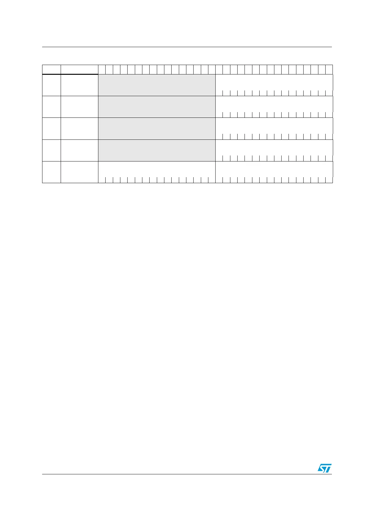
Refer to Table 1 on page 27 for the register boundary addresses.
3Ch
ADC_JDR1
Reserved
JDATA[15:0]
Reset Value 0000000000000000
40h
ADC_JDR2
Reserved
JDATA[15:0]
Reset Value 0000000000000000
44h
ADC_JDR3
Reserved
JDATA[15:0]
Reset Value 0000000000000000
48h
ADC_JDR4
Reserved
JDATA[15:0]
Reset Value 0000000000000000
4Ch
ADC_DR ADC2DATA[15:0] Regular DATA[15:0]
Reset Value 00000000000000000000000000000000
Table 70. ADC - register map and reset values (continued)
Offset Register
31
30
29
28
27
26
25
24
23
22
21
20
19
18
17
16
15
14
13
12
11
10
9
8
7
6
5
4
3
2
1
0
 Loading...


