Datasheet 759
PCI Express* Configuration Registers
19.1.1 VID—Vendor Identification Register
(PCI Express*—D28:F0/F1/F2/F3/F4/F5/F6/F7/F6/F7)
Address Offset: 00h–01h Attribute: RO
Default Value: 8086h Size: 16 bits
19.1.2 DID—Device Identification Register
(PCI Express*—D28:F0/F1/F2/F3/F4/F5/F6/F7/F6/F7)
Address Offset: 02h–03h Attribute: RO
Default Value: Port 1= Bit Description Size: 16 bits
Port 2= Bit Description
Port 3= Bit Description
Port 4= Bit Description
Port 5= Bit Description
Port 6= Bit Description
Port 7= Bit Description
Port 8= Bit Description
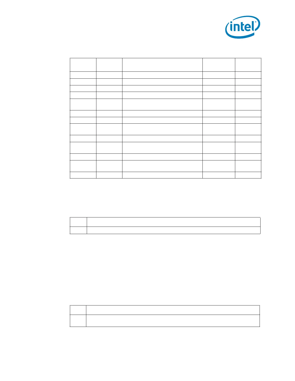
108h–10Bh UEM Uncorrectable Error Mask 00000000h R/WO, RO
10Ch–10Fh UEV Uncorrectable Error Severity 00060011h RO
110h–113h CES Correctable Error Status 00000000h R/WC
114h–117h CEM Correctable Error Mask 00000000h R/WO
118h–11Bh AECC
Advanced Error Capabilities and
Control
00000000h RO
130h–133h RES Root Error Status 00000000h R/WC, RO
180h–183h RCTCL Root Complex Topology Capability List 00010005h RO
184h–187h ESD Element Self Description
See bit
description
RO
190h–193h ULD Upstream Link Description 00000001h RO
198h–19Fh ULBA Upstream Link Base Address
See bit
description
RO
300–303h PECR2 PCI Express Configuration Register 2 60005007h R/W
324–327h PEETM
PCI Express Extended Test Mode
Register
See bit
description
RO
330h–333h PEC1 PCI Express Configuration Register 1 00000000h RO, R/W
Table 19-1. PCI Express* Configuration Registers Address Map
(PCI Express*—D28:F0/F1/F2/F3/F4/F5/F6/F7) (Sheet 3 of 3)
Offset Mnemonic Register Name
Function 0–5
Default
Type
Bit Description
15:0 Vendor ID — RO. This is a 16-bit value assigned to Intel. Intel VID = 8086h
Bit Description
15:0
Device ID — RO. This is a 16-bit value assigned to the PCH’s PCI Express controller.
See the Intel
®
6 Series Chipset Specification Update for the value of the DID Register.
 Loading...