Serial peripheral interface (SPI) UM0306
372/519
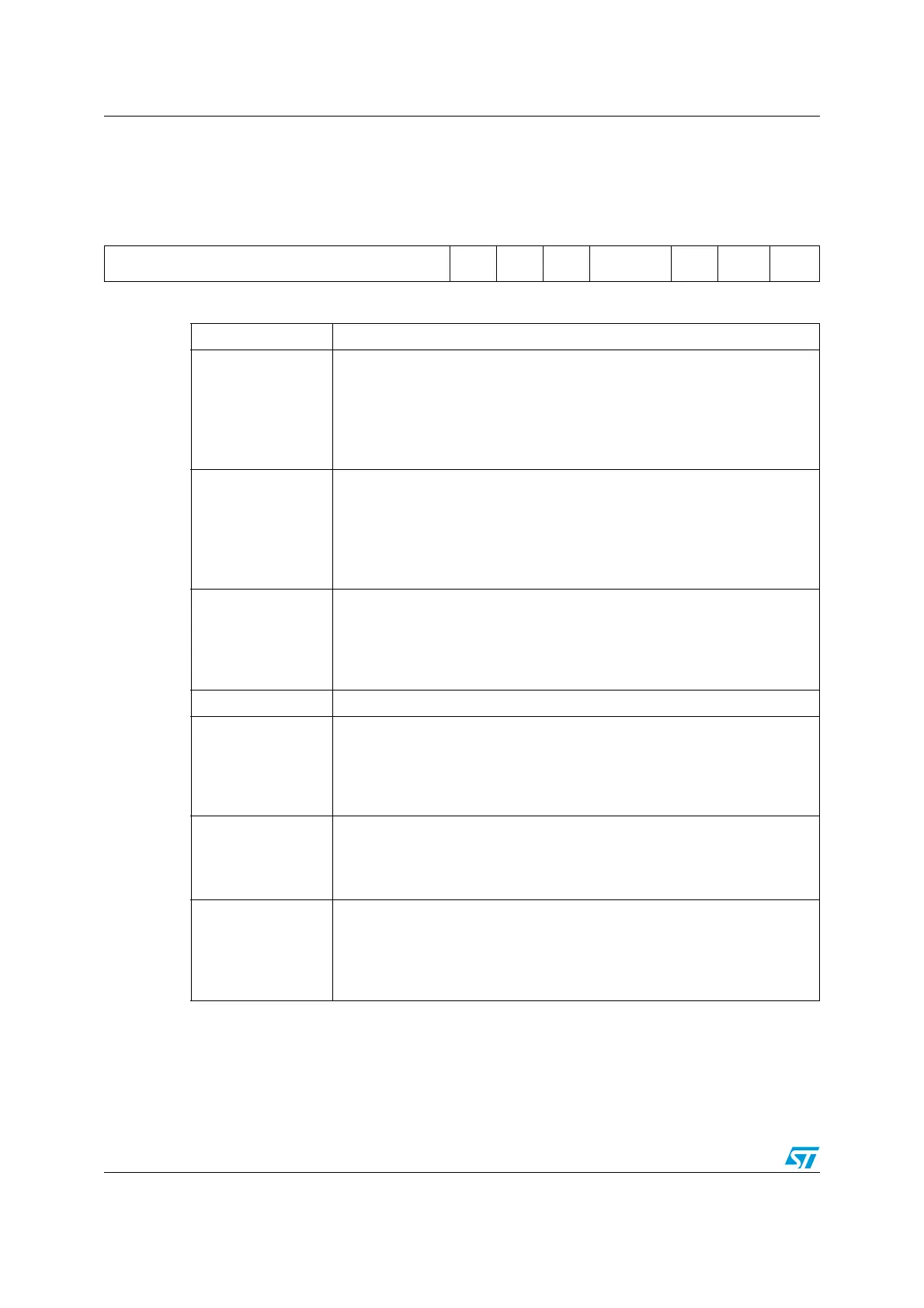
16.4.2 SPI control register 2 (SPI_CR2)
Address Offset: 04h
Reset Value: 0000 0000 (0000h)
15 14 13 12 11 10 9 8 7 6 5 4 3 2 1 0
Reserved TXEIE
RXNE
IE
ERRIE Reserved SSOE
TXDMA
EN
RXDMA
EN
rw rw rw rw rw rw
Bits 15:8 Reserved. Forced to 0 by hardware.
Bit 7
TXEIE: Tx buffer empty interrupt enable
0: TXE interrupt masked
1: TXE interrupt not masked. This allows a interrupt request to be
generated when the TXE flag is set.
Note: To function correctly, the TXEIE and TXDMAEN bits should not be set
at the same time.
Bit 6
RXNEIE: RX buffer not empty interrupt enable
0: RXNE interrupt masked
1: RXNE interrupt not masked. This allows a interrupt request to be
generated when the RXNE flag is set.
Note: To function correctly, the TXEIE and TXDMAEN bits should not be set
at the same time.
Bit 5
ERRIE: Error interrupt enable
This bit controls the generation of an interrupt when an error condition
occurs (CRCERR, OVR, MODF).
0: Error interrupt is masked
1: Error interrupt is enabled.
Bits 4:3 Reserved. Forced to 0 by hardware.
Bit 2
SSOE: SS Output Enable
0: SS output is disabled in master mode and the cell can work in multi-
master configuration
1: SS output is enabled in master mode and when the cell is enabled. The
cell cannot work in a multi-master environment.
Bit 1
TXDMAEN: Tx Buffer DMA Enable
When this bit is set, the DMA request is made whenever the TXE flag is set.
0: Tx buffer DMA disabled
1: Tx buffer DMA enabled
Bit 0
RXDMAEN: Rx Buffer DMA Enable
When this bit is set, the DMA request is made whenever the RXNE flag is
set.
0: Rx buffer DMA disabled
1: Rx buffer DMA enabled
 Loading...


