138 AMCC Proprietary
Revision 1.02 - September 10, 2007
PPC405 Processor
Preliminary User’s Manual
8.3.1 JTAG Connector
A 16-pin male 2x8 header connector is suggested as the JTAG debug port connector. This connector definition
matches the requirements of the RISCWatch debugger. The connector is described in detail in
RISCWatch
Debugger User’s Guide
.
8.3.2 JTAG Instructions
The JTAG debug port provides the standard
extest, idcode, sample/preload, and bypass instructions and the
optional highz and clamp instructions. Invalid instructions behave as the
bypass instruction.
8.3.3 JTAG Boundary Scan
Boundary Scan Description Language (BSDL), IEEE 1149.1b-1994, is a supplement to IEEE 1149.1-1990 and
IEEE 1149.1a-1993
Standard Test Access Port and Boundary-Scan Architecture. BSDL, a subset of the IEEE
1076-1993 Standard VHSIC Hardware Description Language (VHDL), allows a rigorous description of testability
features in components which comply with the standard. BSDL is used by automated test pattern generation tools
for package interconnect tests and by electronic design automation (EDA) tools for synthesized test logic and
verification. BSDL supports robust extensions that can be used for internal test generation and to write software for
hardware debug and diagnostics.
The primary components of BSDL include the logical port description, the physical pin map, the instruction set, and
the boundary register description.
The logical port description assigns symbolic names to the pins of a chip. Each pin has a logical type of in, out,
inout, buffer, or linkage that defines the logical direction of signal flow.
The physical pin map correlates the logical ports of the chip to the physical pins of a specific package. A BSDL
description can have several physical pin maps; each map is given a unique name.
Instruction set statements describe the bit patterns that must be shifted into the Instruction Register to place the
chip in the various test modes defined by the standard. Instruction set statements also support descriptions of
instructions that are unique to the chip.
The boundary register description lists each cell or shift stage of the Boundary Register. Each cell has a unique
number: the cell numbered 0 is the closest to the Test Data Out (TDO) pin; the cell with the highest number is
closest to the Test Data In (TDI) pin. Each cell contains additional information, including: cell type, logical port
associated with the cell, logical function of the cell, safe value, control cell number, disable value, and result value.
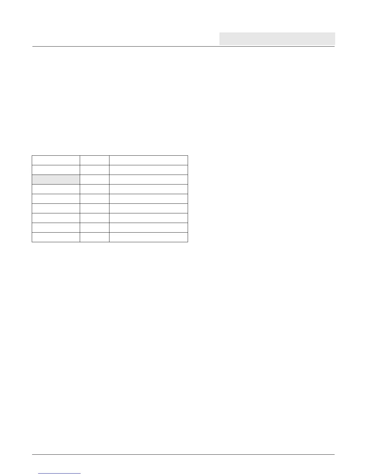
Table 8-1. JTAG Instructions
Instruction Code Comments
Extest 1111000 IEEE 1149.1 standard.
1111001 Reserved.
Sample/Preload 1111010 IEEE 1149.1 standard.
IDCode 1111011 IEEE 1149.1 standard.
Private xxxx100 Private instructions
HighZ 1111101 IEEE 1149.1a-1993 optional
Clamp 1111110 IEEE 1149.1a-1993 optional
Bypass 1111111 IEEE 1149.1 standard.