354 AMCC Proprietary
Revision 1.02 - September 10, 2007
PPC405 Processor
Preliminary User’s Manual
10.5 Special Purpose Registers
Special Purpose Registers (SPRs), which are part of the PowerPC Embedded Environment, are accessed using
the
mtspr and mfspr instructions. SPRs control the use of the debug facilities, timers, interrupts, storage control
attributes, and other architected processor resources.
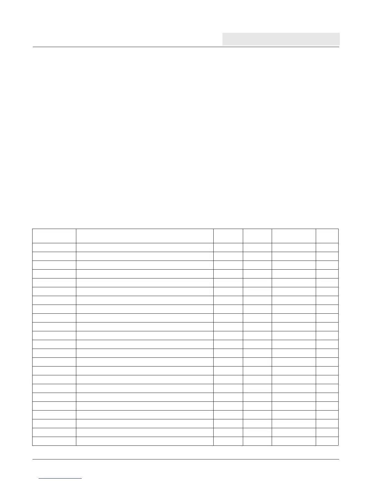
Table 10-3 lists the SPRs, their mnemonics and names, their SPR numbers (SPRNs), and the corresponding
SPRF numbers and access mode. Any SPR numbers that are not listed are reserved and should be neither read
nor written. The columns under the SPRN heading list the register numbers used as operands in assembler
language coding of the
mfspr and mtspr instructions. The column labeled “SPRF” lists the corresponding fields
contained in the machine code of
mfspr and mtspr. The SPRN field contains the five-bit subfields of the SPRF
field, which are reversed in the machine code for the
mfspr and mtspr instructions
(SPRN ← SPRF
5:9
|| SPRF
0:4
) for compatibility with the POWER Architecture. Note that the assembler handles
the special coding transparently.
All SPRs are privileged, except the Count Register (CTR), the Link Register (LR), SPR General Purpose Registers
(SPRG4–SPRG7, read-only), User SPR General Purpose Register (USPRG0), and the Fixed-point Exception
Register (XER). Note that access to the Time Base Lower (TBL) and Time Base Upper (TBU) registers, when
addressed as SPRs, is write-only and privileged. However, when addressed as Time Base Registers (TBRs), read
access to these registers is not privileged. See “Time Base Registers” on page 355. for more information.
Table 10-3. Special Purpose Registers
Mnemonic Register Name SPRN SPRF Access
See
Page
CCR0 Core Configuration Register 0 0x3B3 0x27D Read/Write 77
CTR Count Register 0x009 0x120 Read/Write 36
DAC1 Data Address Compare 1 0x3F6 0x2DF Read/Write 147
DAC2 Data Address Compare 2 0x3F7 0x2FF Read/Write 147
DBCR0 Debug Control Register 0 0x3F2 0x25F Read/Write 143
DBCR1 Debug Control Register 1 0x3BD 0x3BD Read/Write 144
DBSR Debug Status Register 0x3F0 0x21F Read/Clear 145
DCCR Data Cache Cachability Register 0x3FA 0x35F Read/Write 106
DCWR Data Cache Write-through Register 0x3BA 0x35D Read/Write 106
DEAR Data Error Address Register 0x3D5 0x2BE Read/Write 118
DVC1 Data Value Compare 1 0x3B6 0x2DD Read/Write 147
DVC2 Data Value Compare 2 0x3B7 0x2FD Read/Write 147
ESR Exception Syndrome Register 0x3D4 0x29E Read/Write 116
EVPR Exception Vector Prefix Register 0x3D6 0x2DE Read/Write 116
IAC1 Instruction Address Compare 1 0x3F4 0x29F Read/Write 147
IAC2 Instruction Address Compare 2 0x3F5 0x2B5 Read/Write 147
IAC3 Instruction Address Compare 3 0x3B4 0x29D Read/Write 147
IAC4 Instruction Address Compare 4 0x3B5 0x2BD Read/Write 147
ICCR Instruction Cache Cachability Register 0x3FB 0x37F Read/Write 105
ICDBDR Instruction Cache Debug Data Register 0x3D3 0x27E Read-only 80
LR Link Register 0x008 0x100 Read/Write 37
PID Process ID 0x3B1 0x23D Read/Write 102
PIT Programmable Interval Timer 0x3DB 0x37E Read/Write 131