AMCC Proprietary 147
Revision 1.02 - September 10, 2007
PPC405 Processor
Preliminary User’s Manual
8.8.3 Instruction Address Compare Registers (IAC1–IAC4)
The PPC405 can take a debug event upon an attempt to execute an instruction from an address. The address,
which must be word-aligned, is defined in an IAC register. The DBCR0[IA1, IA2] fields of DBCR0 controls the
instruction address compare (IAC) debug event.
8.8.4 Data Address Compare Registers (DAC1–DAC2)
The PPC405 can take a debug event upon storage or cache references to addresses specified in the DAC
registers. The specified addresses in the DAC registers are EAs of operands of storage references or cache
instructions.The fields DBCR1[D1R], [D2R] and DBCR[D1W], [D2W] control the DAC-read and DAC-write debug
events, respectively.
Addresses in the DAC registers specify exact byte EAs for DAC debug events. However, one may want to take a
debug event on any byte within a halfword (ignore the least significant bit (LSb) of the DAC), on any byte within a
word (ignore the two LSbs of DAC), or on any byte within eight words (ignore four LSbs of DAC). DBCR1[D1S,
D2S] control the addressing options.
Errors related to execution of storage reference or cache instructions prevent DAC debug events.
8.8.5 Data Value Compare Registers (DVC1–DVC2)
The PPC405 can take a debug event upon storage or cache references to addresses specified in the DAC
registers, that also require the data at that address to match the value specified in the DVC registers. The data
address compare for a DVC events works the same as for a DAC event. Cache operations do not cause DVC
events. If the data at the address specified matches the value in the corresponding DVC register a DVC event will
occur. The fields DBCR1[DV1M, DV2M] control how the data value are compared.
Errors related to execution of storage reference or cache instructions prevent DVC debug events.
8.8.6 Debug Events
Debug events, enabled and configured by DBCR0 and DBCR1 and recorded in the DBSR, cause debug
operations. A debug event occurs when an event listed in Table 8-2 on page 148 is detected. The debug operation
is performed after the debug event.
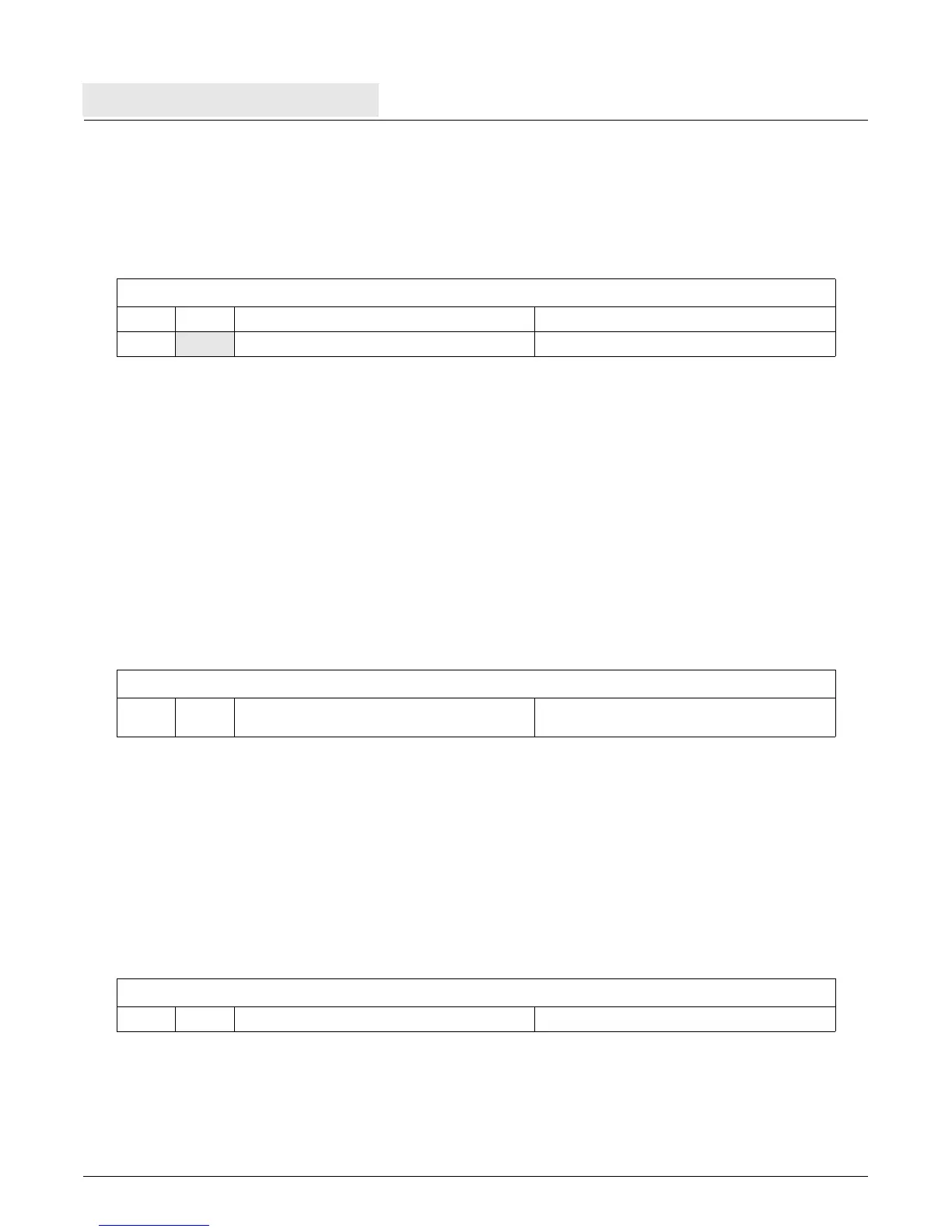
Figure 8-4. Instruction Address Compare Registers (IAC1–IAC4)
0:29 Instruction Address Compare Word Address Omit two low-order bits of complete address.
30:31
Reserved
Figure 8-5. Data Address Compare Registers (DAC1–DAC2)
0:31 Data Address Compare (DAC) Byte Address
DBCR0[D1S] determines which address bits are
examined.
Figure 8-6. Data Value Compare Registers (DVC1–DVC2)
0:31 Data Value to Compare