86 AMCC Proprietary
Revision 1.02 - September 10, 2007
PPC405 Processor
Preliminary User’s Manual
- Data parity generation and checking
- Read/Write protection per bank
• Processor side data port has the highest access priority (maintains predictable memory accesses to the OCM).
4.1 OCM Addressing
The address space for the instruction-side OCM and the data side OCM are defined by the OCM Instruction-Side
Address Range Compare Register (OCM0_ISARC) and OCM Data-Side Address Range Compare Register
(OCM0_DSARC), respectively. These registers are implemented as 6-bit registers that define the most significant
address bits of the respective OCM address space. Using six bits defines a 64MB address space. The instruction
side and data side can share a 64MB address space, or each can have its own 64MB address space. The address
spaces are fully relocatable on 64MB boundaries within the 4GB address space of the PPC405, but the
programmer must assign OCM address space to avoid conflicts with other assigned addresses. See Programming
Model on page 31 for information about the PPC405 memory map.
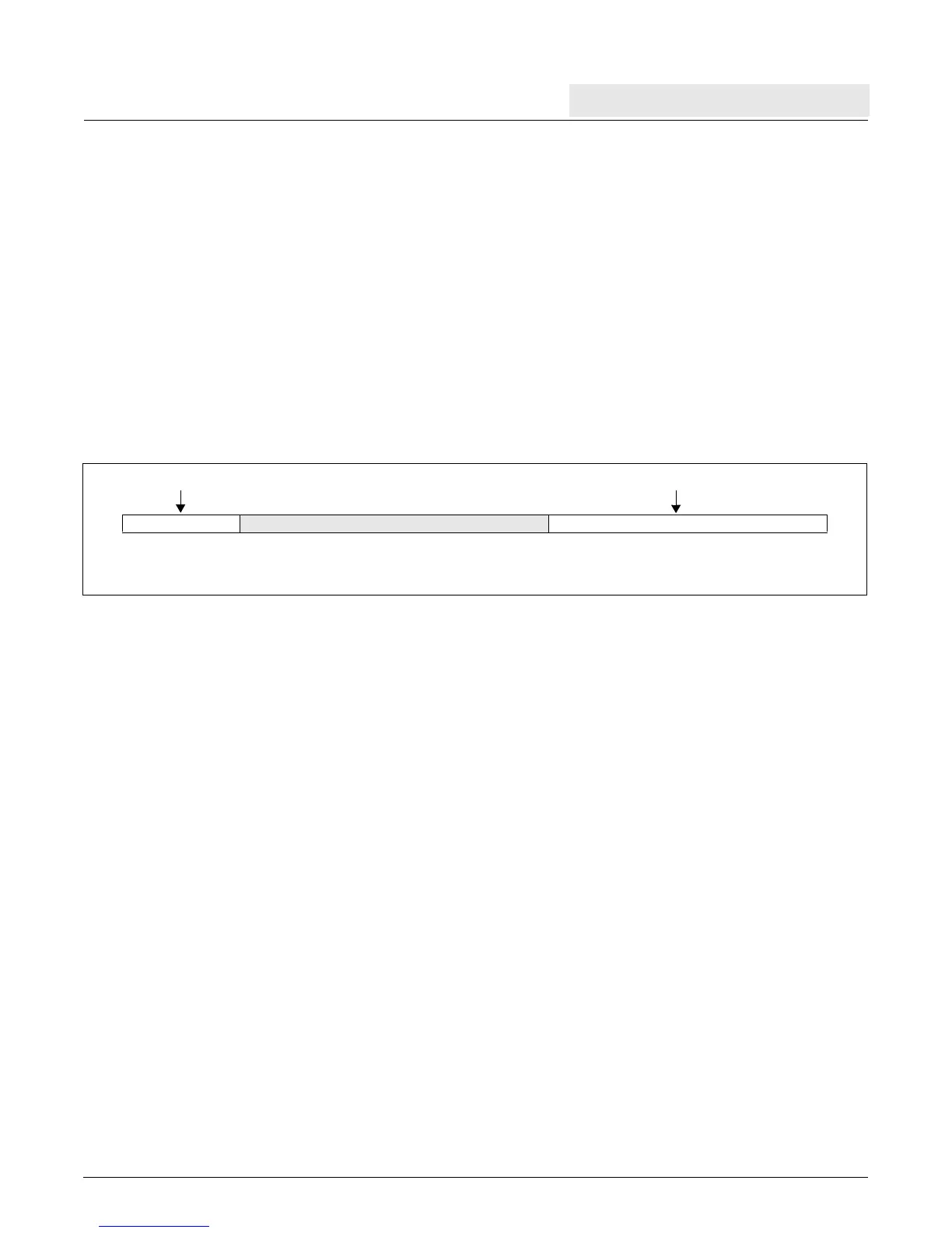
Figure 4-1 illustrates OCM address usage. The OCM SRAM array size is 4KB. Address bits 20:31 select byte
addresses for data-side accesses. Address bits 30:31 are ignored for instruction-side accesses, because
instruction-side accesses return either one or two words per transfer.
Note that the instruction-side and data-side OCM address spaces overlap physically, even if defined as distinct
logical address spaces, because the 4KB SRAM is shared. There is no distinction between data space or
instruction space, except as defined by the programmer.
Addresses in the OCM array are aliased throughout the larger OCM address spaces. The larger OCM address
spaces are filled with multiple images of the 4KB SRAM. Aliased addresses refer to the same physical memory
locations.
Programming Note: To avoid possible memory coherency problems when using aliased addresses, align
aliased addresses on 16KB boundaries rather than on 4KB boundaries. See Store Data Bypass Behavior and
Memory Coherency on page 86 for details.
If address translation is enabled (MSR[IR, DR] = 1), one or more TLB entries for the OCM address space must
exist to validate accesses. However, the virtual addresses are not translated, and 32-bit effective addresses
(virtual addresses) are presented to OCM.
Data-side OCM contents can use big endian or little endian byte ordering. Instruction-side OCM contents must use
big endian byte ordering. See Byte Ordering on page 44 for detailed information about byte ordering.
4.2 Store Data Bypass Behavior and Memory Coherency
The OCM subsystem provides only one mechanism, data-side store operations, for writing both instructions and
data into the OCM array. However, two independent mechanisms request read access of OCM contents; one for
instruction-side fetches and the other for data-side loads.
Figure 4-1. OCM Address Usage
056 19 20 31
OCM Address Space
OCM SRAM