UM10375 All information provided in this document is subject to legal disclaimers. © NXP B.V. 2011. All rights reserved.
User manual Rev. 3 — 14 June 2011 117 of 368
NXP Semiconductors
UM10375
Chapter 7: LPC13xx I/O configuration
7.4.46 IOCON_RI_LOC
Remark: For the LPC1311/01 and LPC1313/01 parts, the modem functions on pins
PIO3_1 to PIO3_3 must be configured in the corresponding IOCONFIG registers and also
in the IOCON_DSR_LOC, IOCON_DCD_LOC, and IOCON_RI_LOC registers (see
Table 140
to Table 101).
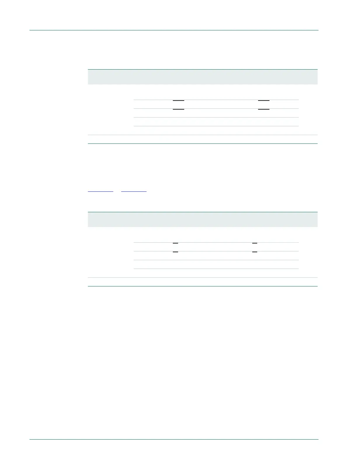
Table 141. IOCON DCD location register (IOCON_DCD_LOC, address 0x4004 40B8) bit
description
Bit Symbol Value Description Reset
value
1:0 DCDLOC Selects pin location for DCD pin (this register is only used for
parts LPC1311/01 and LPC1313/01).
00
0x0 Selects DCD
function in pin location PIO2_2/DCD/MISO1.
0x1 Selects DCD
function in pin location PIO3_2/DCD.
0x2 Reserved.
0x3 Reserved.
31:2 - - Reserved. -
Table 142. IOCON RI location register (IOCON_RI_LOC, address 0x4004 40BC) bit
description
Bit Symbol Value Description Reset
value
1:0 RILOC Selects pin location for RI pin (this register is only used for
parts LPC1311/01 and LPC1313/01)
00
0x0 Selects RI
function in pin location PIO2_3/RI/MOSI1.
0x1 Selects RI
function in pin location PIO3_3/RI.
0x2 Reserved.
0x3 Reserved.
31:2 - - Reserved. -

 Loading...