UM10375 All information provided in this document is subject to legal disclaimers. © NXP B.V. 2011. All rights reserved.
User manual Rev. 3 — 14 June 2011 48 of 368
NXP Semiconductors
UM10375
Chapter 3: LPC13xx System configuration
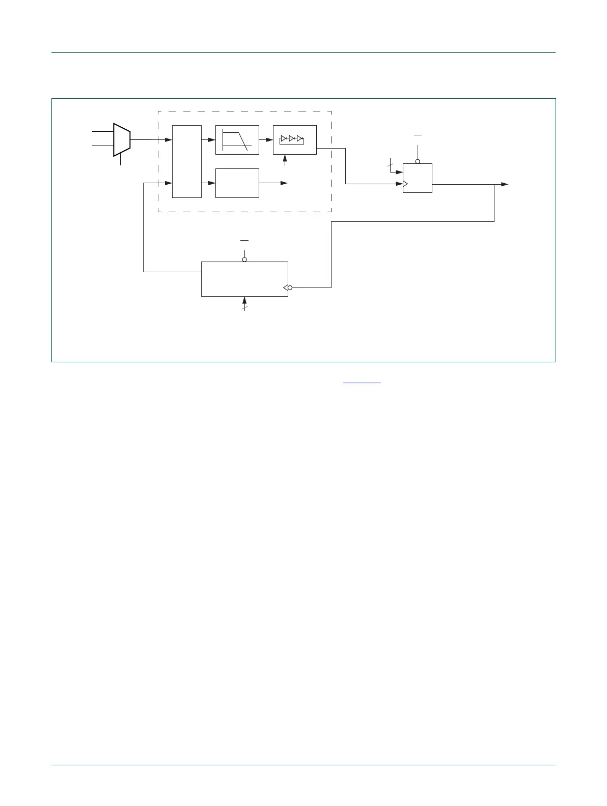
The block diagram of this PLL is shown in Figure 5. The input frequency range is 10 MHz
to 25 MHz. The input clock is fed directly to the Phase-Frequency Detector (PFD). This
block compares the phase and frequency of its inputs, and generates a control signal
when phase and/ or frequency do not match. The loop filter filters these control signals
and drives the current controlled oscillator (CCO), which generates the main clock and
optionally two additional phases. The CCO frequency range is 156 MHz to
320 MHz.These clocks are either divided by 2P by the programmable post divider to
create the output clock(s), or are sent directly to the output(s). The main output clock is
then divided by M by the programmable feedback divider to generate the feedback clock.
The output signal of the phase-frequency detector is also monitored by the lock detector,
to signal when the PLL has locked on to the input clock.
Remark: The divider values for P and M must be selected so that the PLL output clock
frequency FCLKOUT is lower than 100 MHz.
3.11.1 Lock detector
The lock detector measures the phase difference between the rising edges of the input
and feedback clocks. Only when this difference is smaller than the so called “lock
criterion” for more than eight consecutive input clock periods, the lock output switches
from low to high. A single too large phase difference immediately resets the counter and
causes the lock signal to drop (if it was high). Requiring eight phase measurements in a
row to be below a certain figure ensures that the lock detector will not indicate lock until
both the phase and frequency of the input and feedback clocks are very well aligned. This
effectively prevents false lock indications, and thus ensures a glitch free lock signal.
(1) Not on USB PLL.
Fig 5. System and USB PLL block diagram
LOCK
DETECT
PFD
FCLKOUT
pd
analog section
pd
cd
/M
/2P
cd
PSEL<1:0>
pd
2
MSEL<4:0>
5
irc_osc_clk
sys_osc_clk
SYSPLLCLKSEL or
USBPLLCLKSEL
FCLKIN
FCCO
LOCK