UM10375 All information provided in this document is subject to legal disclaimers. © NXP B.V. 2011. All rights reserved.
User manual Rev. 3 — 14 June 2011 123 of 368
NXP Semiconductors
UM10375
Chapter 8: LPC13xx Pin configuration
8.4.1 LQFP48 packages
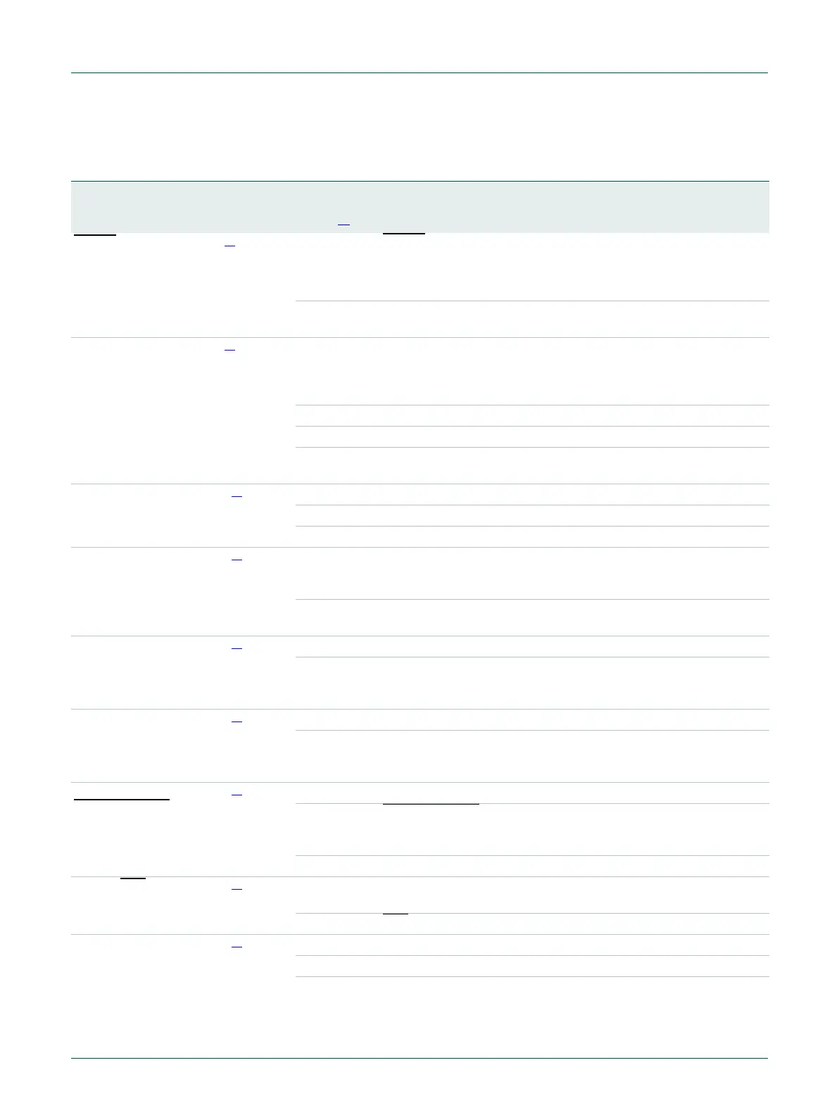
Table 144. LPC1313/42/43 LQFP48 pin description table
Symbol Pin Start
logic
input
Type Reset
state
[1]
Description
RESET
/PIO0_0 3
[2]
yes I I; PU RESET — External reset input with 20 ns glitch filter. A LOW-going
pulse as short as 50 ns on this pin resets the device, causing I/O
ports and peripherals to take on their default states, and processor
execution to begin at address 0.
I/O - PIO0_0 — General purpose digital input/output pin with 10 ns glitch
filter.
PIO0_1/CLKOUT/
CT32B0_MAT2/
USB_FTOGGLE
4
[3]
yes I/O I; PU PIO0_1 — General purpose digital input/output pin. A LOW level on
this pin during reset starts the ISP command handler or the USB
device enumeration (USB on LPC1343 only, see description of
PIO0_3).
O- CLKOUT — Clockout pin.
O- CT32B0_MAT2 — Match output 2 for 32-bit timer 0.
O- USB_FTOGGLE — USB 1 ms Start-of-Frame signal (LPC1343
only).
PIO0_2/SSEL0/
CT16B0_CAP0
10
[3]
yes I/O I; PU PIO0_2 — General purpose digital input/output pin.
I/O - SSEL0 — Slave select for SSP0.
I- CT16B0_CAP0 — Capture input 0 for 16-bit timer 0.
PIO0_3/USB_VBUS 14
[3]
yes I/O I; PU PIO0_3 — General purpose digital input/output pin. LPC1343 only:
A LOW level on this pin during reset starts the ISP command
handler, a HIGH level starts the USB device enumeration.
I- USB_VBUS — Monitors the presence of USB bus power (LPC1343
only).
PIO0_4/SCL 15
[4]
yes I/O I; IA PIO0_4 — General purpose digital input/output pin (open-drain).
I/O - SCL — I
2
C-bus clock input/output (open-drain). High-current sink
only if I
2
C Fast-mode Plus is selected in the I/O configuration
register.
PIO0_5/SDA 16
[4]
yes I/O I; IA PIO0_5 — General purpose digital input/output pin (open-drain).
I/O - SDA — I
2
C-bus data input/output (open-drain). High-current sink
only if I
2
C Fast-mode Plus is selected in the I/O configuration
register.
PIO0_6/
USB_CONNECT
/
SCK0
22
[3]
yes I/O I; PU PIO0_6 — General purpose digital input/output pin.
O- USB_CONNECT
— Signal used to switch an external 1.5 k
resistor under software control. Used with the SoftConnect USB
feature (LPC1343 only).
I/O - SCK0 — Serial clock for SSP0.
PIO0_7/CTS
23
[3]
yes I/O I; PU PIO0_7 — General purpose digital input/output pin (high-current
output driver).
I- CTS
— Clear To Send input for UART.
PIO0_8/MISO0/
CT16B0_MAT0
27
[3]
yes I/O I; PU PIO0_8 — General purpose digital input/output pin.
I/O - MISO0 — Master In Slave Out for SSP0.
O- CT16B0_MAT0 — Match output 0 for 16-bit timer 0.
 Loading...

