UM10375 All information provided in this document is subject to legal disclaimers. © NXP B.V. 2011. All rights reserved.
User manual Rev. 3 — 14 June 2011 208 of 368
NXP Semiconductors
UM10375
Chapter 13: LPC13xx I2C-bus controller
• Data transfer from a master transmitter to a slave receiver. The first byte transmitted
by the master is the slave address. Next follows a number of data bytes. The slave
returns an acknowledge bit after each received byte.
• Data transfer from a slave transmitter to a master receiver. The first byte (the slave
address) is transmitted by the master. The slave then returns an acknowledge bit.
Next follows the data bytes transmitted by the slave to the master. The master returns
an acknowledge bit after all received bytes other than the last byte. At the end of the
last received byte, a “not acknowledge” is returned. The master device generates all
of the serial clock pulses and the START and STOP conditions. A transfer is ended
with a STOP condition or with a Repeated START condition. Since a Repeated
START condition is also the beginning of the next serial transfer, the I
2
C bus will not
be released.
The I
2
C interface is byte oriented and has four operating modes: master transmitter mode,
master receiver mode, slave transmitter mode and slave receiver mode.
The I
2
C interface complies with the entire I
2
C specification, supporting the ability to turn
power off to the ARM Cortex-M3 without interfering with other devices on the same
I
2
C-bus.
13.5.1 I
2
C Fast-mode Plus
Fast-Mode Plus supports a 1 Mbit/sec transfer rate to communicate with the I
2
C-bus
products which NXP Semiconductors is now providing.
In order to use Fast-Mode Plus, the I
2
C pins must be properly configured in the
IOCONFIG register block, see Table 107
and Table 108. In Fast-mode Plus, rates above
400 kHz and up to 1 MHz may be selected.
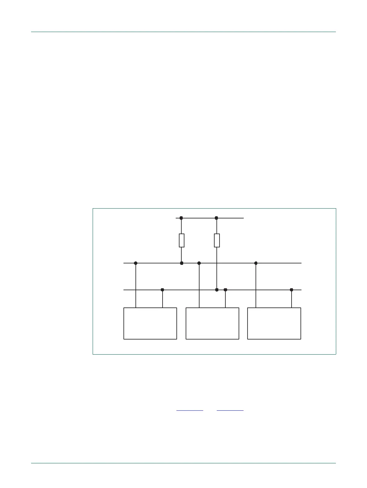
Fig 25. I
2
C-bus configuration
OTHER DEVICE WITH
I
2
C INTERFACE
pull-up
resistor
OTHER DEVICE WITH
I
2
C INTERFACE
LPC13xx
SDA
SCL
I
2
C-bus
SCL
SDA
pull-up
resistor

 Loading...