UM10375 All information provided in this document is subject to legal disclaimers. © NXP B.V. 2011. All rights reserved.
User manual Rev. 3 — 14 June 2011 221 of 368
NXP Semiconductors
UM10375
Chapter 13: LPC13xx I2C-bus controller
13.10.1 Input filters and output stages
Input signals are synchronized with the internal clock, and spikes shorter than three
clocks are filtered out.
The output for I
2
C is a special pad designed to conform to the I
2
C specification.
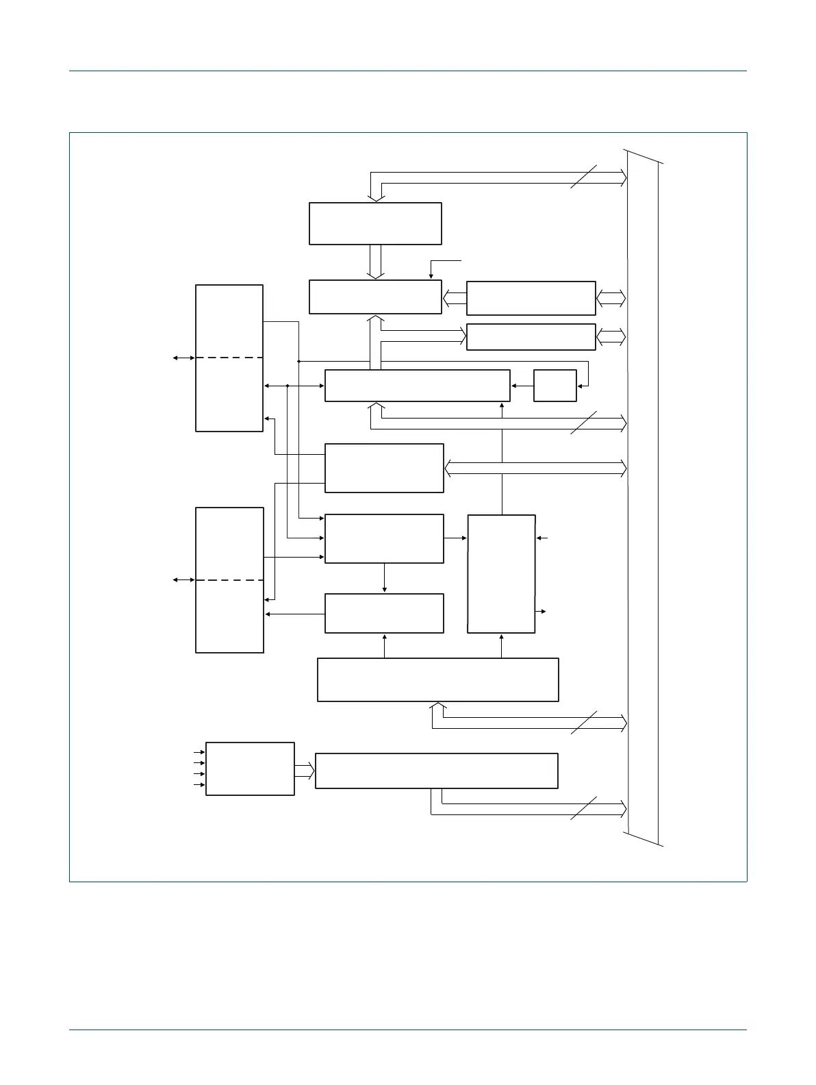
Fig 31. I
2
C serial interface block diagram
APB BUS
STATUS REGISTER
I2CnSTAT
CONTROL REGISTER and
SCL DUTY CYLE REGISTERS
I2CnCONSET, I2CnCONCLR, I2CnSCLH, I2CnSCLL
ADDRESS REGISTERS
MASK and COMPARE
SHIFT REGISTER
I2CnDAT
ACK
BIT COUNTER/
ARBITRATION and
MONITOR MODE
REGISTER
I2CnMMCTRL
SYNC LOGIC
SERIAL CLOCK
GENERATOR
TIMING and
CONTROL
LOGIC
STATUS
DECODER
status
bus
interrupt
PCLK
INPUT
FILTER
OUTPUT
STAGE
SCL
INPUT
FILTER
OUTPUT
STAGE
SDA
I2CnADDR0 to I2CnADDR3
MASK REGISTERS
I2CnMASK0 to I2CnMASK3
I2CnDATABUFFER
MATCHALL
I2CnMMCTRL[3]
8
8
8
16

 Loading...