UM10375 All information provided in this document is subject to legal disclaimers. © NXP B.V. 2011. All rights reserved.
User manual Rev. 3 — 14 June 2011 181 of 368
NXP Semiconductors
UM10375
Chapter 12: LPC13xx UART
[1] LQFP48 packages only.
12.5 Clocking and power control
The clocks and power to the UART block are controlled by two registers:
1. The UART block can be enabled or disabled through the System AHB clock control
register bit 12 (see Table 25
).
2. The UART peripheral clock UART_PCLK is enabled in the UART clock divider
register (see Table 27
). This clock is used by the UART baud rate generator.
Remark: For LPC1311/13/42/43 parts, the UART pins must be configured in the
corresponding IOCON registers before the UART clocks are enabled. For the
LPC1311/01 and LPC1313/01 parts, no special enabling sequence is required.
12.6 Register description
The UART contains registers organized as shown in Table 193. The Divisor Latch Access
Bit (DLAB) is contained in U0LCR[7] and enables access to the Divisor Latches.
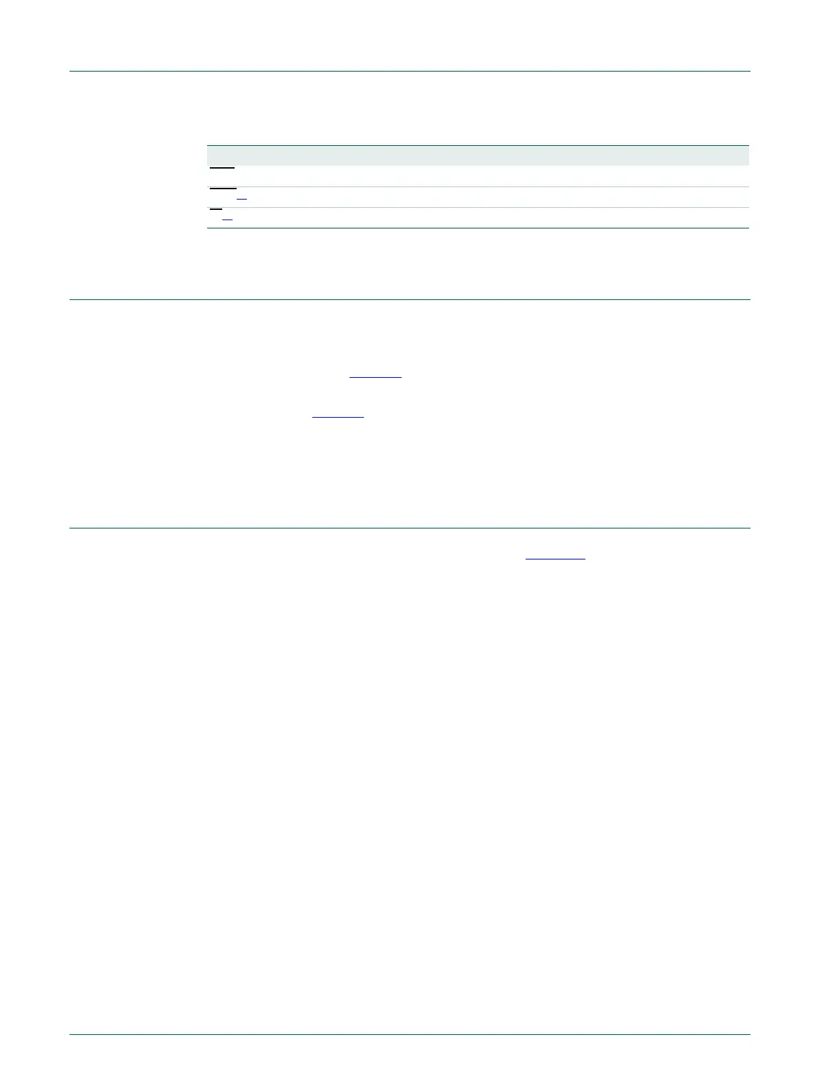
CTS Input Clear To Send.
DCD
[1]
Input Data Carrier Detect.
RI
[1]
Input Ring Indicator.
Table 192. UART pin description
Pin Type Description

 Loading...
