UM10375 All information provided in this document is subject to legal disclaimers. © NXP B.V. 2011. All rights reserved.
User manual Rev. 3 — 14 June 2011 12 of 368
NXP Semiconductors
UM10375
Chapter 3: LPC13xx System configuration
3.3 Pin description
Table 6 shows pins that are associated with system control block functions.
[1] For HVQFN packages, applies to P2_0, P3_2, and P3_3 only.
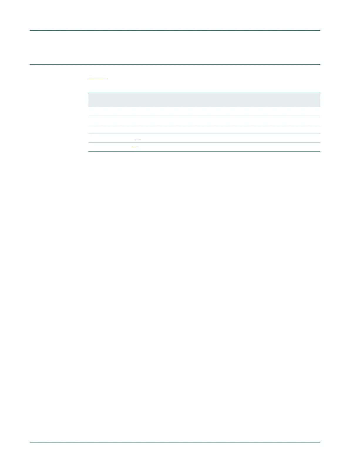
Table 6. Pin summary
Pin name Pin
direction
Pin description
CLKOUT O Clockout pin
PIO0_0 to PIO0_11 I Wake-up pins port 0
PIO1_0 to PIO1_11 I Wake-up pins port 1
PIO2_0 to PIO2_11
[1]
I Wake-up pins port 2
PIO3_0 to PIO3_3
[1]
I Wake-up pins port 3
 Loading...

