UM10375 All information provided in this document is subject to legal disclaimers. © NXP B.V. 2011. All rights reserved.
User manual Rev. 3 — 14 June 2011 15 of 368
NXP Semiconductors
UM10375
Chapter 3: LPC13xx System configuration
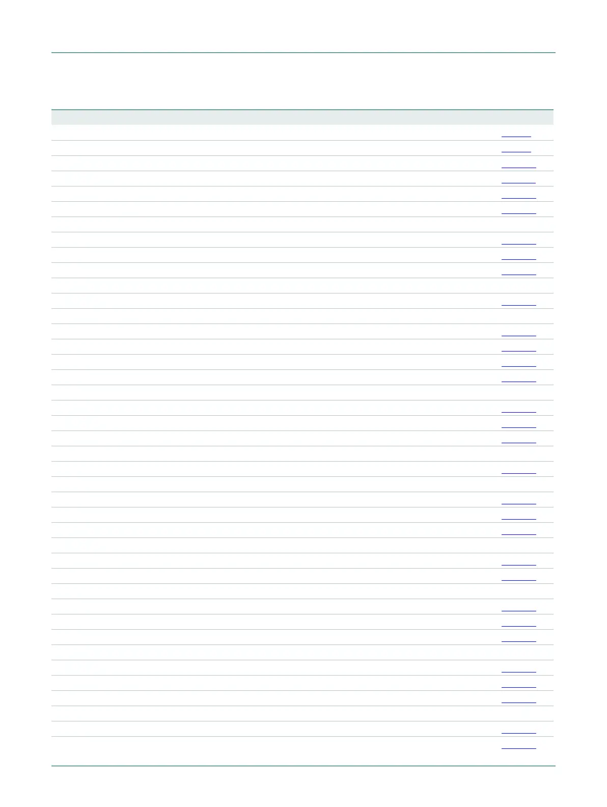
Table 7. Register overview: system control block (base address 0x4004 8000)
Name Access Address offset Description Reset value Reference
SYSMEMREMAP R/W 0x000 System memory remap 0x0000 0002 Table 8
PRESETCTRL R/W 0x004 Peripheral reset control 0x0000 0000 Table 9
SYSPLLCTRL R/W 0x008 System PLL control 0x0000 0000 Table 10
SYSPLLSTAT R 0x00C System PLL status 0x0000 0000 Table 11
USBPLLCTRL R/W 0x010 USB PLL control 0x0000 0000 Table 12
USBPLLSTAT R 0x014 USB PLL status 0x0000 0000 Table 13
- - 0x018 - 0x01C Reserved - -
SYSOSCCTRL R/W 0x020 System oscillator control 0x0000 0000 Table 14
WDTOSCCTRL R/W 0x024 Watchdog oscillator control 0x0000 0000 Table 15
IRCCTRL R/W 0x028 IRC control 0x0000 0080 Table 16
- - 0x02C Reserved - -
SYSRESSTAT R 0x030 System reset status register 0x0000 0000 Table 17
- - 0x034 - 0x03C Reserved - -
SYSPLLCLKSEL R/W 0x040 System PLL clock source select 0x0000 0000 Table 18
SYSPLLCLKUEN R/W 0x044 System PLL clock source update enable 0x0000 0000 Table 19
USBPLLCLKSEL R/W 0x048 USB PLL clock source select 0x0000 0000 Table 20
USBPLLCLKUEN R/W 0x04C USB PLL clock source update enable 0x0000 0000 Table 21
- - 0x050 - 0x06C Reserved - -
MAINCLKSEL R/W 0x070 Main clock source select 0x0000 0000 Table 22
MAINCLKUEN R/W 0x074 Main clock source update enable 0x0000 0000 Table 23
SYSAHBCLKDIV R/W 0x078 System AHB clock divider 0x0000 0001 Table 24
- - 0x07C Reserved - -
SYSAHBCLKCTRL R/W 0x080 System AHB clock control 0x0000 485F Table 25
- - 0x084 - 0x090 Reserved - -
SSP0CLKDIV R/W 0x094 SSP0 clock divider 0x0000 0000 Table 26
UARTCLKDIV R/W 0x098 UART clock divder 0x0000 0000 Table 27
SSP1CLKDIV R/W 0x09C SSP1 clock divider 0x000 Table 28
- - 0x0A0 - 0x0A8 Reserved - -
TRACECLKDIV R/W 0x0AC ARM trace clock divider 0x0000 0000 Table 29
SYSTICKCLKDIV R/W 0x0B0 SYSTICK clock divder 0x0000 0000 Table 30
- - 0x0B4 - 0x0BC Reserved - -
USBCLKSEL R/W 0x0C0 USB clock source select 0x0000 0000 Table 31
USBCLKUEN R/W 0x0C4 USB clock source update enable 0x0000 0000 Table 32
USBCLKDIV R/W 0x0C8 USB clock source divider 0x0000 0000 Table 33
- - 0x0CC Reserved - -
WDTCLKSEL R/W 0x0D0 WDT clock source select 0x0000 0000 Table 34
WDTCLKUEN R/W 0x0D4 WDT clock source update enable 0x0000 0000 Table 35
WDTCLKDIV R/W 0x0D8 WDT clock divider 0x0000 0000 Table 36
- - 0x0DC Reserved - -
CLKOUTCLKSEL R/W 0x0E0 CLKOUT clock source select 0x0000 0000 Table 37
CLKOUTUEN R/W 0x0E4 CLKOUT clock source update enable 0x0000 0000 Table 38
 Loading...

