UM10375 All information provided in this document is subject to legal disclaimers. © NXP B.V. 2011. All rights reserved.
User manual Rev. 3 — 14 June 2011 14 of 368
NXP Semiconductors
UM10375
Chapter 3: LPC13xx System configuration
3.5 Register description
All registers, regardless of size, are on word address boundaries. Details of the registers
appear in the description of each function.
See Section 3.12
for the flash access timing register, which can be re-configured as part
the system setup. This register is not part of the system configuration block.
USB is available in parts LPC134x only.
SSP1 is available on part LPC1313FBD48 only.
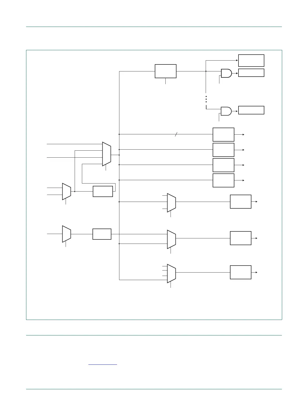
Fig 3. LPC13xx CGU block diagram
SYS PLL
irc_osc_clk
sys_osc_clk
sys_osc_clk
wdt_osc_clk
irc_osc_clk
irc_osc_clk
wdt_osc_clk
USB PLL
MAINCLKSEL
SYSPLLCLKSEL
USBPLLCLKSEL
CLOCK
DIVIDER
SYSAHBCLKCTRL
(ROM enable)
SYSAHBCLKCTRL
(SSP1 enable)
CLOCK
DIVIDER
SSP0/1_PCLK
CLOCK
DIVIDER
UART_PCLK
CLOCK
DIVIDER
CLOCK
DIVIDER
SYSTICK
timer
CLOCK
DIVIDER
ARM trace clock
WDCLK
WDTUEN
CLOCK
DIVIDER
usb_clk
USBUEN
wdt_osc_clk
irc_osc_clk
sys_osc_clk
CLOCK
DIVIDER
CLKOUT
CLKOUTUEN
main clock system clock
sys_pllclkin
usb_pllclkin
sys_pllclkout
usb_pllclkout
2
ARM
CORTEX-M3
ROM
SSP1
SYSAHBCLKDIV
 Loading...

